Page 197 - Build Your Own Transistor Radios a Hobbyists Guide to High-Performance and Low-Powered Radio Circuits
P. 197

+9                      +5
                                                            C24
                                           C2           lo01 ut
                                    rT  47 pr      R7                                      Re
                                 33 U~     R3      3,3K                   J 0,0047uf       lK     R9    100
                   Long Wire Antenna
               I                           47                   U1 B  74HC4066      U2B    C9    100K   C1l

                    T1
             C15    21F129   LowSide Tap   R16          2N3906                             1 ut        33~T
            .01  uf  t                    2                                   C5
               ~:                                       R6           0,0047 u~                         I Output
                                                        100
                                       100
                                                                 U'l C  74HC4066
                                                       R5
                                                                     0.0047 u;f;    +9
                                               R4      22                     C6
                                               470                             Cl0         Rl0
                                                                          ~Uf              lK
                                                                     U1D
                                                                 I                               Rl1
                                                                  74HC4066
                                                                                            CB
                                                                  1                              100K
                                                                 I    /0  11
                  o Degree Phase                                  12                       1 ut
                                                                                                       C13   -  --
                                                                                                       33~T
                  180 Degrees Phase
                  90 Degrees Phase
                                                                                                      Q Output
                  270 Degrees Phase
                                                                     Note: U2 and U3 are NE5532 or LM833
                           To Ground D3 ToC3
                                           2  To Base of 01
                              ToC15  4     1  ToClIRl
                                  T1  Bottom  Side
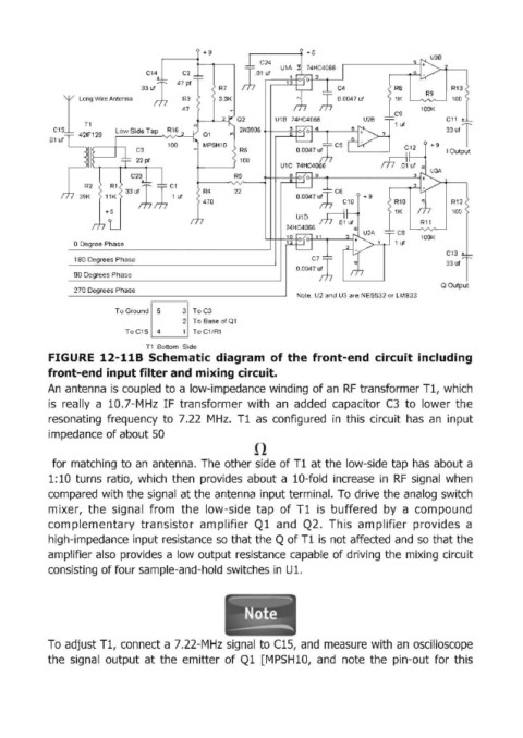
            FIGURE  12-118 Schematic  diagram  of the front-end  circuit including

            front-end input filter and mixing circuit.
            An  antenna  is  coupled  to a low-impedance winding  of an  RF transformer Tl, which
            is  really  a  lO.7-MHz  I F transformer  with  an  added  capacitor  C3  to  lower  the
            resonating  frequency  to  7.22  MHz.  Tl  as  configured  in  this circuit  has  an  input

            impedance of about 50


             for matching  to an  antenna.  The  other side  of T1  at the  low-side  tap  has  about a
            l: 10  turns  ratio,  which  then  provides  about  a  lD-fold  increase  in  RF  signal when
            compared  with the signal  at the antenna  input terminal.  To drive the analog  switch
            mixer,  the  signa'l  from  the  low-side  tap  of Tl  is  buffered  by  a  compound
            comp lementary  transistor  amplifier  Ql  and  Q2.  This  amplifier  provides  a
            high-impedance input resistance so that the Q of Tl is  not affected and  so  that the

            amplifier also  provides  a low output resistance capable  of driving the mixing  circuit
            consisting of four sample-and-hold switches in Ul.


            To adjust Tl, connect a 7.22-MHz signal to C1S,  and  measure  with  an  oscilloscope
            the  signal  output  at the  emitter  of Ql  [MPSHlD,  and  note  the  pin-out  for  this
   192   193   194   195   196   197   198   199   200   201   202