Page 214 - Build Your Own Transistor Radios a Hobbyists Guide to High-Performance and Low-Powered Radio Circuits
P. 214
The output voltage then will  be about 156 mV  x  0.312  x  0.038  x  2,700 = 5.0 volts

            peak.  Note  that  0.312  x  0.038  = G ml  the  large-signal  transconductance,  which  is
            smaller  than  the  small-signal  transconductance  by  a  multiplying  factor  of about
            0.312.
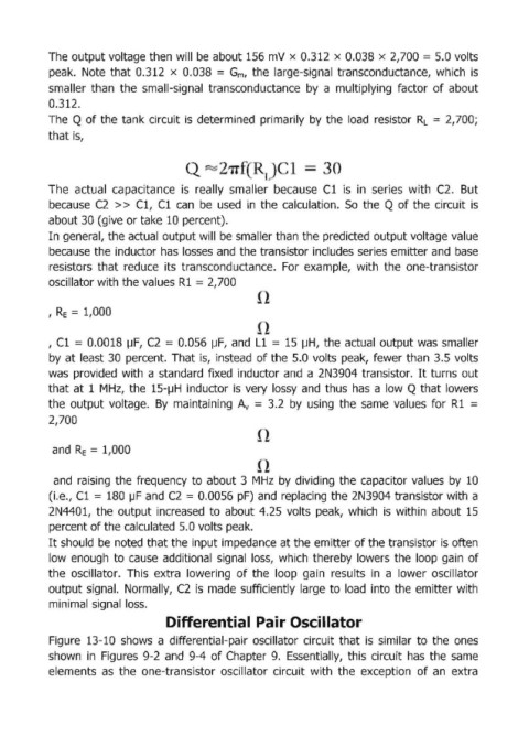
            The  Q of the  tank circuit  is  determined  primarily  by  the  load  resistor  RL  = 2,700;
            that is,


                                                             L
            The  actual  capacitance  is  really  smaller  because  Cl  is  in  series  with  C2.  But
            because  C2  »  Cl,  Cl  can  be  used  in  the  calculation.  So  the  Q of the  circuit  is
            about 30 (give or take 10 percent).

            In general, the actual output will  be smaller than the predicted output voltage value
            because the inductor has losses and  the transistor includes series emitter and  base
            resistors  that  reduce  its  transconductance.  For  example,  with  the  one-transistor
            oscillator with the values R1  = 2,700


            , RE  = 1,000


            , Cl = 0.0018  IJF,  C2  = 0.056  IJF,  and  L1  = 15  IJH,  the actual  output was  smaller
            by  at least 30  percent.  That is,  instead  of the  5.0  volts  peak,  fewer than  3.5  volts
            was  provided  with  a standard  fixed  inductor and  a 2N3904 transistor.  It turns  out
            that at  1 MHz,  the  15-~H inductor is  very  lossy  and  thus  has  a  low Q  that lowers
            the  output  voltage.  By  maintaining  Av  =  3.2  by  using  the  same  values  for  R1  =

            2,700


             and  RE  = 1,000


             and  raising  the  frequency  to  about 3 ,MHz  by  dividing  the  capacitor  values  by  10

            (i.e.,  Cl = 180  IJF  and  C2  = 0.0056 pF)  and  replacing  the  2N3904 transistor with a
            2N4401,  the  output  increased  to  about 4.25  volts  peak,  which  is  within  about  15
            percent of the calculated  5.0 volts peak.
            It should  be  noted that the input impedance at the emitter of the transistor is often
            low  enough  to  cause  additional  signal  loss,  which  thereby  lowers  the  loop  gain  of
            the  oscillator.  This  extra  lowering  of the  loop  gain  results  in  a  lower  oscillator

            output signal.  Normally,  C2  is  made  sufficiently  large to  load  into the emitter with
            minimal signal loss.
                                      Differential Pair Oscillator

            Figure  13-10  shows  a  differential-pair  oscillator  circuit  that  is  similar  to  the  ones
            shown  in  Figures  9-2  and  9-4  of Chapter  9.  Essentially,  this  circuit  has  the  same
            elements  as  the  one-transistor  oscillator  circuit  with  the  exception  of an  extra

