Page 36 - CNC Robotics
P. 36

Chapter 2 / Electronics


             L297-1297D

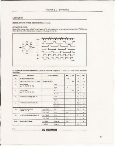
             MOTOR DRIVING PHASE SEQUENCES (continued)
             WAVE DRIVE MODE
             Wave drive mode (also called "one-phase-on" drive) is selected by a low level on the HALF/F'O[[ input
             when the translatoris at an even numbered state (2, 4, 6 or 8).


                                   """
                     m   ""  G:i        ....n     n        n        r
                                              n        n        n...-

                                        -II          n        n
                                        -,
                                   0
                         0\00
                                   "'"
                                   ""
                                                                   t ·....


             ELECTRICAL CHARACTERISTICS (Refer to the block diagram Tamb = 25"C, V s = 5V unless otherwise
             specified)
             Symbo l      Param eter          Testcondltlons  Min.  Typ  Max.  Uni t
               V,  Supply voltage (pin 12)                    4.75       7    V
                   Qui escent supply current (pin 12)  Outpu ts float ing  50  BO  mA
               "
               V,  Input voltage                   l ow                  0.6  V
                   (pin 11,17,18, 19, 20)
                                                   High        2         V,   V
               "   Input current                   Vj", L           ' 00  pA
                   (pin 11, 17, 18, 19, 20)
                                                   VI""H                 10   pA
               V~  Enable input voltage (pin 10j   low                   1.3  V
                                                   High        2         V,   V
               ~ ,  Enable inp ut cu rren t (pin 10)  V....'" L          100  pA
                                                   V en ", H             10   pA
               v;  Phase outpu t voltage  I" =l OmA  V",-                OA   V
                   (pins 4, 6, 7, 9)
                                        1 0 = 5mA  VOH         3.9            V
               V,nll  Inhibit output voltage (pins 5, 8)  1 0= 10mA  ViM L  OA  V
                                        1 0 = SmA  Vir>h H     3.9            V
              VSYNC  Sync Output Voltage  1 0 = SmA  VSYNC H   3.3            V
                                        1 0 = 5mA  VSYNCv                O.B
             6111


                                                                                              27
   31   32   33   34   35   36   37   38   39   40   41