
Page 521 - Cam Design Handbook
P. 521
THB15 9/19/03 8:03 PM Page 509
CAMS IN MICROELECTROMECHANICAL SYSTEMS 509
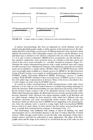
FIGURE 15.1. A simple cantilever example to illustrate the surface micromachining process.
In surface micromachining, thin films are deposited on a thick substrate wafer and
etched using photolithographic masks to define patterns in the deposited layers. By alter-
nating deposition and etching, several layers of different materials can be stacked to create
intricate microstructures. Since lithography requires flat surfaces and the thickness of an
individual layer is limited to a few microns compared to the size of the wafers (usually 2,
3, 4, 6, 8, and 12 inches in diameter), MEMS devices are generally very flat structures. In
this sandwich construction, some sacrificial layers are included so that they can be dis-
solved at the end to create releasable (i.e., movable) mechanical structures. Figure 15.1
illustrates the surface micromachining process with a single sacrificial layer and a single
movable structural layer. Multilayered structures with alternating structural and sacrificial
layers can be obtained in a similar manner. MUMPs, Multi-User MEMS Processes, which
were successfully made available as a foundry process for MEMS by the Microelectronic
Center of North Carolina, is an example of a multilayered surface micromachining process.
SUMMiT, Sandia Ultra-planar Multi-level MEMS Technology,* process is another
example. While MUMPs consisted of three structural layers, SUMMiT consists of four or
five with added steps of planarization in between. Many of the devices described in Sec.
5 of this chapter are made using the SUMMiT process.
In contrast to surface micromachining, in bulk micromachining a bulk wafer whose
thickness is of the order of a few hundred microns is sculpted using etching techniques to
define the structures. Bulk micromachining also uses deposition and etching of thin films,
but the primary feature creation is due to the substantial etching of the substrate wafer.
When etched through large depths, the distinction between isotropic and anisotropic etches
becomes important. Some chemicals etch certain materials equally in all directions and
are called isotropic etchants for those materials, while others have different etch rates
in different directions and create anisotropically etched surfaces. Both isotropic and
anisotropic etches are effectively used in MEMS devices depending on the desired geom-
etry. Since the substrate wafer is etched to a large depth, bulk micromachined MEMS
devices tend to be much (about 10 times) thicker than the surface micromachined struc-
tures. A sample bulk micromachining technique is illustrated in Fig. 15.2.
One disadvantage with traditional bulk etching of silicon in building very thick
microstructures (up to a few hundred microns) is the lack of vertical sidewalls of etched
surfaces. While isotropic etches lead to curved sidewalls, some anisotropic etches lead to
slanted surfaces, and both are undesirable in many applications. The shape of the litho-
graphic mask and the shape of the etched pit as viewed from the top of the wafer are also
*Sandia National Laboratory, www.mems.sandia.gov