
Page 522 - Cam Design Handbook
P. 522
THB15 9/19/03 8:03 PM Page 510
510 CAM DESIGN HANDBOOK
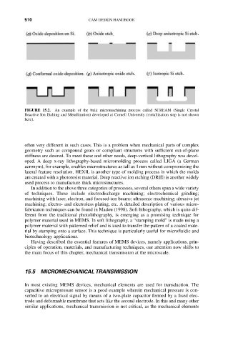
a . b . c .
d . e . f .
FIGURE 15.2. An example of the bulk micromachining process called SCREAM (Single Crystal
Reactive Ion Etching and Metallization) developed at Cornell University (metallization step is not shown
here).
often very different in such cases. This is a problem when mechanical parts of complex
geometry such as compound gears or compliant structures with sufficient out-of-plane
stiffness are desired. To meet these and other needs, deep-vertical lithography was devel-
oped. A deep x-ray lithography-based micromolding process called LIGA (a German
acronym), for example, enables microstructures as tall as 1mm without compromising the
lateral feature resolution. HEXIL is another type of molding process in which the molds
are created with a photoresist material. Deep reactive ion etching (DRIE) is another widely
used process to manufacture thick microstructures.
In addition to the above three categories of processes, several others span a wide variety
of techniques. These include electrodischarge machining; electrochemical grinding;
machining with laser, electron, and focused-ion beams; ultrasonic machining; abrasive jet
machining; electro- and electroless plating, etc. A detailed description of various micro-
fabricaton techniques can be found in Madou (1998). Soft lithography, which is quite dif-
ferent from the traditional photolithography, is emerging as a promising technique for
polymer material used in MEMS. In soft lithography, a “stamping mold” is made using a
polymer material with patterned relief and is used to transfer the pattern of a coated mate-
rial by stamping onto a surface. This technique is particularly useful for microfluidic and
biotechnology applications.
Having described the essential features of MEMS devices, namely applications, prin-
ciples of operation, materials, and manufacturing techniques, our attention now shifts to
the main focus of this chapter, mechanical transmission at the microscale.
15.5 MICROMECHANICAL TRANSMISSION
In most existing MEMS devices, mechanical elements are used for transduction. The
capacitive micropressure sensor is a good example wherein mechanical pressure is con-
verted to an electrical signal by means of a two-plate capacitor formed by a fixed elec-
trode and deformable membrane that acts like the second electrode. In this and many other
similar applications, mechanical transmission is not critical, as the mechanical elements