
Page 265 - Chalcogenide Glasses for Infrared Optics
P. 265
240 Cha pte r Ni ne
Using an expression by Moss that allows for changing the wave-
25
length dependency, we were able to estimate values of about 67 per-
cent of observed values in contrast to only 40 percent for classical
expressions. The conclusion reached was that a GaAs window doped
to 10 Ω·cm would provide sufficient EMI protection with little effect
on the 8- to 12-µm transmission.
To demonstrate the merits of forming large plates using the hori-
zontal Bridgman, AMI made one last plate 12 in × 6 in × 1 in, undoped
and high-resistivity. The beginning of transmission started at about
0.8 µm and was fully transmitting by 1.5 µm. Transmission at the Yag
1.064 µm was 40 percent uncorrected; with antireflection coating it
−1
would be 73 percent. The calculated absorption coefficient was 0.48 cm .
The plate would be a very good window 1.5 to 14 µm and still useful
for the Yag laser. Transmission values, measured at six locations, of
2.5 to 25 µm were identical with no absorption over the range except
for a small intrinsic absorption occurring at 13 µm.
AMI decided to attack the other point of criticism directed at
GaAs— resistance to rain erosion. Earlier, it was mentioned that silicon
had the best physical properties for an infrared window material next
to sapphire. One criticism leveled against the material was a weak
−1
(0.8 cm absorption coefficient) broad intrinsic band occurring at about
9 µm. Silicon containing oxygen as an impurity places an additional
absorption band peaked at 9 µm due to the presence of oxygen as an
impurity. The SiO absorption may add an additional amount of absorp-
tion, reaching a total value of 8 cm at the oxygen saturation level of
−1
18
2 × 10 atoms. However, as pointed out earlier, silicon may be made
oxygen-free by vacuum float zoning, and thus only the weak intrinsic
band would not be much of an absorption problem for silicon in thin
pieces, such as 1 to 2 mm. AMI decided that a GaAs window could be
protected from rain erosion damage if it was coated with a silicon layer.
Also, common semiconductor techniques could be used to provide con-
ducting grid patterns in the surface useful for EMI protection or even for
window deicing. The concept of protecting GaAs windows with a layer
of silicon is contained in U.S. Patent 5,194,985 granted to AMI in 1993.
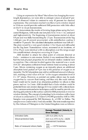
Samples were prepared by Bill Herrmann, Jr., of OEC in Dallas. The
samples were coated with a 3-mil silicon film. The tests results reported
by Des Gibson of Pilkington in the United Kingdom were as follows:
Damage Threshold (Velocity to
Show Damage)
Untreated GaAs 130 m/s (291 mi/h)
Silicon-protected GaAs 210 m/s (470 mi/h) + 162%
improvement hardness
950
Ratio of measured silicon/GaAs =+167% hardness
575