
Page 274 - Chalcogenide Glasses for Infrared Optics
P. 274
Early Work at Texas Instruments 249
(< 1-µm) region but become quite different in the infrared as the
wavelength increases. The same statement is true for other semicon-
ductor processes such as Ge on Ge or GaAs on GaAs. For N-type silicon,
the absorption by conduction electrons increases by the square of the
3–5
wavelength. The result is strong reflection at the layer substrate
interface without which optical interference would not occur. Reflec-
tivity R at the interface between two dielectric materials with index
values of N and N is given by
2 1
( N − N ) 2
R = 2 1
( N + N ) 2
2 1
However, for a material with strong absorption the index becomes a
complex number N = N – ik, where k is the imaginary part; the extinction
−1
coefficient calculated from α= 4πk/λ with α in cm units is the linear
absorption coefficient calculated from transmission measured at the
wavelength λ. In general, working with transparent materials, k is
so small it is ignored. But in this case, calculation of R at the silicon-
dielectric interface with absorbing silicon becomes more complicated:
( n − n ) 2 + k 2
R = 2 1 2
12 n + 2 + 2
( n ) k
2 1 2
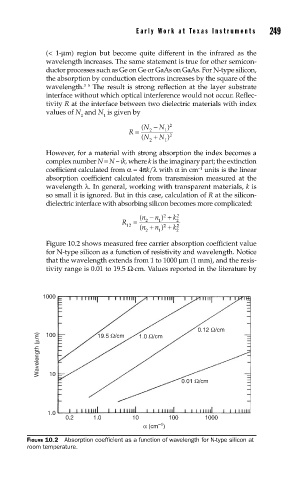
Figure 10.2 shows measured free carrier absorption coefficient value
for N-type silicon as a function of resistivity and wavelength. Notice
that the wavelength extends from 1 to 1000 µm (1 mm), and the resis-
tivity range is 0.01 to 19.5 Ω·cm. Values reported in the literature by
1000
0.12 Ω/cm
100
Wavelength (µm)
19.5 Ω/cm
1.0 Ω/cm
10
0.01 Ω/cm
1.0
0.2 1.0 10 100 1000
–1
α (cm )
FIGURE 10.2 Absorption coeffi cient as a function of wavelength for N-type silicon at
room temperature.