
Page 102 - Complete Wireless Design
P. 102
Amplifier Design
Amplifier Design 101
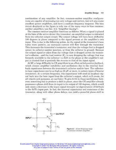
combination of any amplifier. In fact, common-emitter amplifier configura-
tions are capable of increasing not only voltage and current, but will also make
excellent power amplifiers, and have a medium-frequency response. The bias
circuit displayed in the figure is only one of the many ways to bias common-
emitter amplifiers (see Sec. 3.3, “Amplifier biasing”).
The common-emitter amplifier functions as follows: When a signal is placed
at the base of the active device (the transistor), an amplified output is extracted
from the collector output circuit. The output voltage will have been shifted by
180 degrees in phase compared to the signal present at the amplifier’s own
input. This is due to the following action. As the signal at the transistor’s base
turns more positive, an increased current will flow through the transistor.
This decreases the transistor’s resistance, and thus the voltage that is dropped
across its collector-emitter junction, or from the collector to ground. Because
the output signal is taken from the voltage that is dropped across the transis-
tor’s collector—and the load resistor (R ) is now dropping the voltage that was
C
formerly available to the collector—a shift in the phase at the amplifier’s out-
put is created that is precisely the reverse to that of the input signal.
At RF, a large difficulty in CE amplifiers is an effect called positive feedback,
which creates amplifier instability and oscillations due to the internal feed-
back capacitance between the transistor’s collector and its base. The collector-
to-base capacitance can be as high as 25 pF, or more, in certain types of bipolar
transistors. At a certain frequency, this capacitance will send an in-phase sig-
nal back into the base input from the collector’s output, which will create, for
all intents and purposes, an oscillator. To give birth to these oscillations, how-
ever, something has to produce a shift in phase, since the CE amplifier already
possesses a phase shift from its input to its output of 180 degrees, which would
only cause a decrease in the input signal strength (or degeneration) if fed back
to the BJT’s input port. In fact, the internal capacitance and resistance of the
transistor, along with other phase delays, can yield a powerful phase shift to
Figure 3.3 A low-frequency type
of common-emitter amplifier.
Downloaded from Digital Engineering Library @ McGraw-Hill (www.digitalengineeringlibrary.com)
Copyright © 2004 The McGraw-Hill Companies. All rights reserved.
Any use is subject to the Terms of Use as given at the website.