
Page 104 - Complete Wireless Design
P. 104
Amplifier Design
Amplifier Design 103
Unlike the common-emitter amplifier, the CC amplifier has no phase inver-
sion between its input and output, since the current through the active device
will increase as the input signal to the transistor’s base rises in amplitude.
This action forces a rise in the current through the emitter resistor, which
increases the voltage drop across R , resulting in a 0 degree phase shift.
E
Most common-collector amplifiers do not possess any voltage-robbing collec-
tor resistor, nor do they use an R bypass capacitor, which would also lower the
E
output voltage at V .
OUT
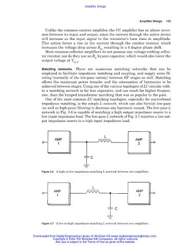
Matching networks. There are numerous matching networks that can be
employed to facilitate impedance matching and coupling, and supply some fil-
tering (normally of the low-pass variety) between RF stages as well. Matching
allows the maximum power transfer and the attenuation of harmonics to be
achieved between stages. Using one of the various topologies of LC circuits with-
in a matching network is far less expensive, and can reach far higher frequen-
cies, than the lumped transformer matching that was so popular in the past.
One of the most common LC matching topologies, especially for narrowband
impedance matching, is the simple L network, which can also furnish low-pass
(as well as high-pass) filtering to decrease any harmonic output. The low-pass L
network in Fig. 3.6 is capable of matching a high output impedance source to a
low input impedance load. The low-pass L network of Fig. 3.7 matches a low out-
put impedance source to a high input impedance load.
Figure 3.6 A high-to-low impedance-matching L network between two amplifiers.
Figure 3.7 A low-to-high impedance-matching L network between two amplifiers.
Downloaded from Digital Engineering Library @ McGraw-Hill (www.digitalengineeringlibrary.com)
Copyright © 2004 The McGraw-Hill Companies. All rights reserved.
Any use is subject to the Terms of Use as given at the website.