
Page 103 - Complete Wireless Design
P. 103
Amplifier Design
102 Chapter Three
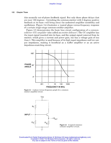
this normally out-of-phase feedback signal. But only those phase delays that
are near 180 degrees—furnishing the common-emitter with 0 degrees positive
feedback at its base—will bring about the undesired amplifier instability and
oscillations. Figure 3.4 illustrates a typical phase-versus-frequency response
of a certain single-stage common-emitter amplifier.
Figure 3.5 demonstrates the basic bias circuit configuration of a common-
collector (CC) amplifier (also called an emitter-follower). The CC amplifier has
the input signal inserted into its base, and the output signal removed from its
emitter; which gives a current and power gain, but has a voltage gain of less
than 1. This amplifier is used because of its high input impedance and low out-
put impedance, making it beneficial as a buffer amplifier or as an active
impedance-matching circuit.
Figure 3.4 A phase-versus-frequency graph for a common-
emitter amplifier circuit.
Figure 3.5 A typical common-
collector amplifier circuit.
Downloaded from Digital Engineering Library @ McGraw-Hill (www.digitalengineeringlibrary.com)
Copyright © 2004 The McGraw-Hill Companies. All rights reserved.
Any use is subject to the Terms of Use as given at the website.