
Page 11 - Complete Wireless Design
P. 11
Wireless Essentials
10 Chapter One
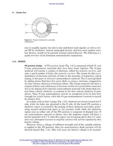
Figure 1.8 Proper winding for a toroidal
transformer.
only to amplify signals, but also to mix and detect such signals, as well as cre-
ate RF by oscillation. Indeed, integrated circuits, and thus most modern wire-
less devices, would not be possible without semiconductors. The following is a
quick overview of the dominant semiconductor components.
1.2.2 DIODES
PN junction diodes. A PN junction diode (Fig. 1.9) is composed of both N- and
P-type semiconductor materials that have been fused together. The N-type
material will contain a surplus of electrons, called the majority carriers, and
only a small number of holes, the minority carriers. The reason for this over-
abundance of electrons and lack of holes is the insertion of impurities, called
doping, to the pure (or intrinsic) semiconductor material. This is accomplished
by adding atoms that have five outer shell, or valence, electrons, compared to
the four valence electrons of intrinsic silicon. The P-type material will have a
surplus of holes and a deficiency of electrons within its crystal lattice structure
due to the doping of the intrinsic semiconductor material with atoms that con-
tain three valence electrons, in contrast to the four valence electrons of pure
silicon. Thus, P-type semiconductor current is considered to be by hole flow
through the crystal lattice, while the N-type semiconductor’s current is caused
by electron flow.
In a diode with no bias voltage (Fig. 1.10), electrons are drawn toward the P
side, while the holes are attracted to the N side. At the fused PN junction a
depletion region is created by the joining of these electrons and holes, gener-
ating neutral electron-hole pairs at the junction itself; while the depletion
region area on either side of the PN junction is composed of charged ions. If
the semiconductor material is silicon, then the depletion region will have a
barrier potential of 0.7 V, with this region not increasing above this 0.7 value
since any attempted increase in majority carriers will now be repulsed by this
barrier voltage.
However, when a voltage of sufficient strength and of the suitable polarity
is applied to the PN junction, then the semiconductor diode junction will be
forward biased (Fig. 1.11). This will cause the barrier voltage to be neutral-
Downloaded from Digital Engineering Library @ McGraw-Hill (www.digitalengineeringlibrary.com)
Copyright © 2004 The McGraw-Hill Companies. All rights reserved.
Any use is subject to the Terms of Use as given at the website.