
Page 12 - Complete Wireless Design
P. 12
Wireless Essentials
Wireless Essentials 11
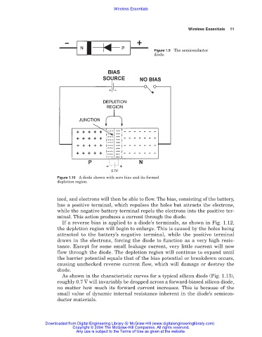
Figure 1.9 The semiconductor
diode.
Figure 1.10 A diode shown with zero bias and its formed
depletion region.
ized, and electrons will then be able to flow. The bias, consisting of the battery,
has a positive terminal, which repulses the holes but attracts the electrons,
while the negative battery terminal repels the electrons into the positive ter-
minal. This action produces a current through the diode.
If a reverse bias is applied to a diode’s terminals, as shown in Fig. 1.12,
the depletion region will begin to enlarge. This is caused by the holes being
attracted to the battery’s negative terminal, while the positive terminal
draws in the electrons, forcing the diode to function as a very high resis-
tance. Except for some small leakage current, very little current will now
flow through the diode. The depletion region will continue to expand until
the barrier potential equals that of the bias potential or breakdown occurs,
causing unchecked reverse current flow, which will damage or destroy the
diode.
As shown in the characteristic curves for a typical silicon diode (Fig. 1.13),
roughly 0.7 V will invariably be dropped across a forward-biased silicon diode,
no matter how much its forward current increases. This is because of the
small value of dynamic internal resistance inherent in the diode’s semicon-
ductor materials.
Downloaded from Digital Engineering Library @ McGraw-Hill (www.digitalengineeringlibrary.com)
Copyright © 2004 The McGraw-Hill Companies. All rights reserved.
Any use is subject to the Terms of Use as given at the website.