
Page 111 - Complete Wireless Design
P. 111
Amplifier Design
110 Chapter Three
When an amplifier is below its P1dB, then for every 1-dB increase in fun-
damental power into the amplifier, the output second-order products will
increase by 2 dB, while the output third-order products will increase by 3 dB.
The reverse is also true: For every 1 dB decrease in the fundamental input
power, the second and third orders decrease in power by 2 and 3 dB, respec-
tively. However, by increasing the desired input signals, there will reach some
point where the third-order products must be (theoretically) equal to the fun-
damental outputs. This is the third-order intercept point (TOIP).
The third-order intercept point is approximately 10 to 15 dB above the P1dB
compression point. The TOIP is the point where, when two different (but close-
ly spaced in frequency) input signals are placed at the amplifier’s input port,
the undesired output third-order products will be at the same amplitude as the
desired two-tone fundamental input signals. However, the output TOIP itself
can never actually be reached. This is because the amplifier will go into satu-
ration before this amplitude is ever truly attained. Even though Fig. 3.13 does
not show it, the third-order product’s output power will gain-limit, just as the
fundamental signal must, when the amplifier goes into saturation.
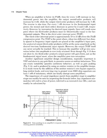
Another significant amplifier design consideration, especially important in
VHF and above in any gain block, is excessive source or emitter inductance. This
can create instability (possible oscillatory behavior), as well as gain peaking
(Fig. 3.14), and is produced by using an emitter resistor in the amplifier design.
It is made worse by the addition of the emitter resistor’s own bypass capacitor,
long emitter leads, and even long vias to ground (even SMD chip capacitors can
have 1 nH of inductance, which can fatally disrupt some amplifiers).
The importance of a good impedance match from amplifier stage to amplifier
stage can readily be seen by inspecting the formula below. Any impedance mis-
matches will end in a loss of power, referred to as mismatch loss (ML), and can
readily be calculated by:
Figure 3.14 Gain peaking in an amplifier’s response (above its passband),
causing general instability.
Downloaded from Digital Engineering Library @ McGraw-Hill (www.digitalengineeringlibrary.com)
Copyright © 2004 The McGraw-Hill Companies. All rights reserved.
Any use is subject to the Terms of Use as given at the website.