
Page 84 - Complete Wireless Design
P. 84
Modulation
Modulation 83
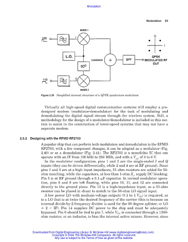
Figure 2.36 Simplified internal structure of a QPSK quadrature modulator.
Virtually all high-speed digital communication systems will employ a pre-
designed modem (modulator-demodulator) for the task of modulating and
demodulating the digital signal stream through the wireless system. Still, a
methodology for the design of a modulator/demodulator is included in this sec-
tion to assist in the construction of lower-speed systems that may not have a
separate modem.
2.5.2 Designing with the RFMD RF2703
A popular chip that can perform both modulation and demodulation is the RFMD
RF2703; with a few component changes, it can be adopted as a modulator (Fig.
2.40) or as a demodulator (Fig. 2.41). The RF2703 is a monolithic IC that can
operate with an IF from 100 kHz to 250 MHz, and with a V of 3 to 6 V.
CC
In the modulator configuration, pins 1 and 3 are the single-ended I and Q
inputs (they can be driven differentially, while 2 and 4 are at RF ground). Since
pins 1 and 3 are at a high input impedance, 51-ohm resistors are added for 50-
ohm matching, while the capacitors, at less than 1-ohm X , supply DC blocking.
c
Pin 5 is at RF ground through a 0.1-
F capacitor. In normal modulator opera-
tion, pins 8 and 9 are left floating, while pins 10, 11, and 12 are connected
directly to the ground plane. Pin 13 is a high-impedance input, so a 51-ohm
resistor can be placed in shunt to match to the 50-ohm LO signal input.
A low power LO with medium-voltage outputs (0.1 to 1 V ) is required, as
PP
is a LO that is at twice the desired frequency of the carrier (this is because an
internal divide-by-2 frequency divider is used for the 90 degree splitter; or LO
2 IF). Pin 14 supplies DC power to the chip and must be adequately
bypassed. Pin 6 should be tied to pin 7, while V CC is connected through a 1200-
ohm resistor, or an inductor, to bias the internal active mixers. However, since
Downloaded from Digital Engineering Library @ McGraw-Hill (www.digitalengineeringlibrary.com)
Copyright © 2004 The McGraw-Hill Companies. All rights reserved.
Any use is subject to the Terms of Use as given at the website.