
Page 86 - Complete Wireless Design
P. 86
Modulation
Modulation 85
Figure 2.38 A signal’s phase states through a
quadrature modulator in the time domain.
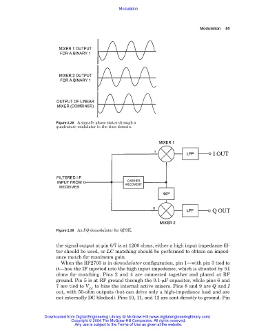
Figure 2.39 An I/Q demodulator for QPSK.
the signal output at pin 6/7 is at 1200 ohms, either a high input impedance fil-
ter should be used, or LC matching should be performed to obtain an imped-
ance match for maximum gain.
When the RF2703 is in demodulator configuration, pin 1—with pin 3 tied to
it—has the IF injected into the high input impedance, which is shunted by 51
ohms for matching. Pins 2 and 4 are connected together and placed at RF
ground. Pin 5 is at RF ground through the 0.1-
F capacitor, while pins 6 and
7 are tied to V to bias the internal active mixers. Pins 8 and 9 are Q and I
CC
out, with 50-ohm outputs (but can drive only a high-impedance load and are
not internally DC blocked). Pins 10, 11, and 12 are sent directly to ground. Pin
Downloaded from Digital Engineering Library @ McGraw-Hill (www.digitalengineeringlibrary.com)
Copyright © 2004 The McGraw-Hill Companies. All rights reserved.
Any use is subject to the Terms of Use as given at the website.