Page 86 -
P. 86
2.3 The digital camera                                                                  65


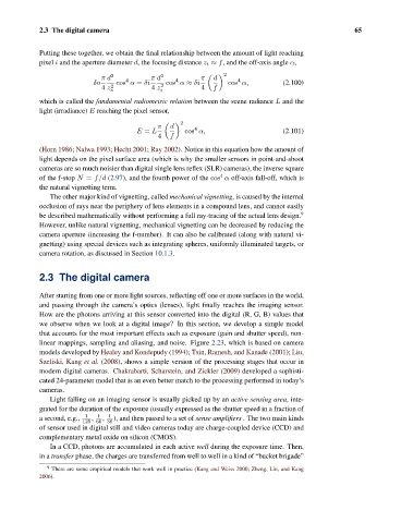
               Putting these together, we obtain the final relationship between the amount of light reaching
               pixel i and the aperture diameter d, the focusing distance z i ≈ f, and the off-axis angle α,
                                 π d 2  4      π d 2  4     π      2   4
                                                                d
                              δo     cos α = δi    cos α ≈ δi       cos α,         (2.100)
                                 4 z o 2       4 z 2 i       4  f
               which is called the fundamental radiometric relation between the scene radiance L and the
               light (irradiance) E reaching the pixel sensor,

                                                       2
                                                π   d
                                                           4
                                           E = L        cos α,                     (2.101)
                                                4   f
               (Horn 1986; Nalwa 1993; Hecht 2001; Ray 2002). Notice in this equation how the amount of
               light depends on the pixel surface area (which is why the smaller sensors in point-and-shoot
               cameras are so much noisier than digital single lens reflex (SLR) cameras), the inverse square
                                                                  4
               of the f-stop N = f/d (2.97), and the fourth power of the cos α off-axis fall-off, which is
               the natural vignetting term.
                  The other major kind of vignetting, called mechanical vignetting, is caused by the internal
               occlusion of rays near the periphery of lens elements in a compound lens, and cannot easily
               be described mathematically without performing a full ray-tracing of the actual lens design. 9
               However, unlike natural vignetting, mechanical vignetting can be decreased by reducing the
               camera aperture (increasing the f-number). It can also be calibrated (along with natural vi-
               gnetting) using special devices such as integrating spheres, uniformly illuminated targets, or
               camera rotation, as discussed in Section 10.1.3.


               2.3 The digital camera

               After starting from one or more light sources, reflecting off one or more surfaces in the world,
               and passing through the camera’s optics (lenses), light finally reaches the imaging sensor.
               How are the photons arriving at this sensor converted into the digital (R, G, B) values that
               we observe when we look at a digital image? In this section, we develop a simple model
               that accounts for the most important effects such as exposure (gain and shutter speed), non-
               linear mappings, sampling and aliasing, and noise. Figure 2.23, which is based on camera
               models developed by Healey and Kondepudy (1994); Tsin, Ramesh, and Kanade (2001); Liu,
               Szeliski, Kang et al. (2008), shows a simple version of the processing stages that occur in
               modern digital cameras. Chakrabarti, Scharstein, and Zickler (2009) developed a sophisti-
               cated 24-parameter model that is an even better match to the processing performed in today’s
               cameras.
                  Light falling on an imaging sensor is usually picked up by an active sensing area, inte-
               grated for the duration of the exposure (usually expressed as the shutter speed in a fraction of
               a second, e.g.,  1  ,  1  ,  1  ), and then passed to a set of sense amplifiers . The two main kinds
                           125  60  30
               of sensor used in digital still and video cameras today are charge-coupled device (CCD) and
               complementary metal oxide on silicon (CMOS).
                  In a CCD, photons are accumulated in each active well during the exposure time. Then,
               in a transfer phase, the charges are transferred from well to well in a kind of “bucket brigade”

                  9  There are some empirical models that work well in practice (Kang and Weiss 2000; Zheng, Lin, and Kang
               2006).

