
Page 296 - DSP Integrated Circuits
P. 296
7.3 FFT Processor, Cont. 281
ware modules step by step, starting from the algorithm. We begin by partitioning
the algorithm, followed by scheduling, resource allocation, resource assignment,
and finally, synthesis of a matching architecture. We will first perform a crude
design, then subsequently improve it until a satisfactory solution is reached.
7.3.1 First Design Iteration
In a top-down design approach we start by identifying the major tasks (processes)
to be executed. The aim is to successively describe the whole DSP system as a hier-
archy of communicating processes. In practice, it is important that the system
description can be executed in order to validate its correctness. High-level lan-
guages such as VHDL can be used for this purpose. Unfortunately, many conven-
tional languages such as Pascal and C are unsuitable for this purpose due to a lack
of static variables between procedure calls.
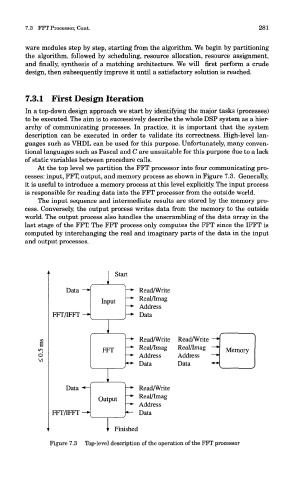
At the top level we partition the FFT processor into four communicating pro-
cesses: input, FFT, output, and memory process as shown in Figure 7.3. Generally,
it is useful to introduce a memory process at this level explicitly. The input process
is responsible for reading data into the FFT processor from the outside world.
The input sequence and intermediate results are stored by the memory pro-
cess. Conversely, the output process writes data from the memory to the outside
world. The output process also handles the unscrambling of the data array in the
last stage of the FFT. The FFT process only computes the FFT since the IFFT is
computed by interchanging the real and imaginary parts of the data in the input
and output processes.
Figure 7.3 Top-level description of the operation of the FFT processor