Page 297 - DSP Integrated Circuits
P. 297
282                                             Chapter 7 DSP System Design

            These processes are then partitioned into a hierarchy of simpler processes.
        Partitioning should be performed such that the processes at the lowest level in the
        hierarchy can be easily mapped onto hardware resources. Both the input and out-
        put processes are simple processes needing little further refinement. The parti-
        tioning should be done in steps where each step is sufficiently small as to make the
        transformation obvious, thereby avoiding design errors.


        Resource Allocation
        Next we determine the resources required. The partitioning assumes that the
        input, FFT, and output processes are executed sequentially. It is possible to over-
        lap their execution and speed up the FFT processor slightly, but the complexity of
        the design would increase significantly. The number of butterfly operations for
        each FFT is


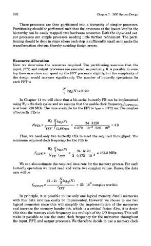
            In Chapter 11 we will show that a bit-serial butterfly PE can be implemented
        using Wd = 24 clock cycles and we assume that the usable clock frequency, fcLPEmax*
        is at least 220 MHz. The time available for the FFT is t FFT = 0.372 ms. The number
        of butterfly PEs is


            Thus, we need only two butterfly PEs to meet the required throughput. The
        minimum required clock frequency for the PEs is


            We can also estimate the required data rate for the memory process. For each
        butterfly operation we must read and write two complex values. Hence, the data
        rate will be


            In principle, it is possible to use only one logical memory. Small memories
        with this data rate can easily be implemented. However, we choose to use two
        logical memories since this will simplify the implementation of the memories
        and increase the memory bandwidth, which is a critical factor. Also, it is desir-
        able that the memory clock frequency is a multiple of the I/O frequency. This will
        make it possible to use the same clock frequency for the memories throughout
        the input, FFT, and output processes. We therefore decide to use a memory clock

