
Page 30 - DSP Integrated Circuits
P. 30
1.6 DSP System Design 15
(i.e., processing elements, memories, and communication channels) must be allo-
cated to implement the system. Another important problem in this design phase is
to assign each operation to a resource on which it will be executed. The next design
step involves synthesis of a suitable architecture with the appropriate number of
processing elements, memories, and communication channels or selection of a
standard (ASIC) signal processor. In the former case, the amount of resources as
well as the control structure can be derived from the schedule. The implementa-
tion cost depends strongly on the chosen target architecture. This design step will
be discussed in Chapters 8 and 9.
The last step in the system design phase involves logic design of the func-
tional blocks in the circuit architecture [1, 14]. The result of the system design
phase is a complete description of the system and subsystems down to the transis-
tor level.
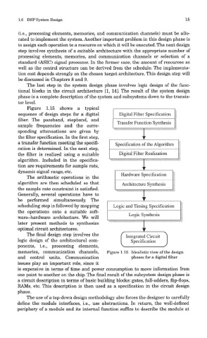
Figure 1.15 shows a typical
sequence of design steps for a digital
filter. The passband, stopband, and
sample frequencies and the corre-
sponding attenuations are given by
the filter specification. In the first step,
a transfer function meeting the specifi-
cation is determined. In the next step,
the filter is realized using a suitable
algorithm. Included in the specifica-
tion are requirements for sample rate,
dynamic signal range, etc.
The arithmetic operations in the
algorithm are then scheduled so that
the sample rate constraint is satisfied.
Generally, several operations have to
be performed simultaneously. The
scheduling step is followed by mapping
the operations onto a suitable soft-
ware-hardware architecture. We will
later present methods to synthesize
optimal circuit architectures.
The final design step involves the
logic design of the architectural com-
ponents, i.e., processing elements,
memories, communication channels, Figure 1.15 Idealistic view of the design
and control units. Communication phases for a digital filter
issues play an important role, since it
is expensive in terms of time and power consumption to move information from
one point to another on the chip. The final result of the subsystem design phase is
a circuit description in terms of basic building blocks: gates, full-adders, flip-flops,
RAMs, etc. This description is then used as a specification in the circuit design
phase.
The use of a top-down design methodology also forces the designer to carefully
define the module interfaces, i.e., use abstractions. In return, the well-defined
periphery of a module and its internal function suffice to describe the module at