
Page 262 - Electrical Properties of Materials
P. 262
244 Dielectric materials
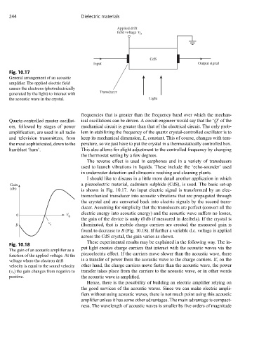
Applied drift
field voltage V
0
CdS
Input Output signal
Fig. 10.17
General arrangement of an acoustic
amplifier. The applied electric field
causes the electrons (photoelectrically
Transducer
generated by the light) to interact with
the acoustic wave in the crystal. Light
frequencies that is greater than the frequency band over which the mechan-
Quartz-controlled master oscillat- ical oscillations can be driven. A circuit engineer would say that the ‘Q’ofthe
ors, followed by stages of power mechanical circuit is greater than that of the electrical circuit. The only prob-
amplification, are used in all radio lem in stabilizing the frequency of the quartz crystal-controlled oscillator is to
and television transmitters, from keep its mechanical dimension, L, constant. This of course, changes with tem-
the most sophisticated, down to the perature, so we just have to put the crystal in a thermostatically controlled box.
humblest ‘ham’. This also allows for slight adjustment to the controlled frequency by changing
the thermostat setting by a few degrees.
The reverse effect is used in earphones and in a variety of transducers
used to launch vibrations in liquids. These include the ‘echo-sounder’ used
in underwater detection and ultrasonic washing and cleaning plants.
I should like to discuss in a little more detail another application in which
Gain a piezoelectric material, cadmium sulphide (CdS), is used. The basic set-up
(db)
is shown in Fig. 10.17. An input electric signal is transformed by an elec-
tromechanical transducer into acoustic vibrations that are propagated through
the crystal and are converted back into electric signals by the second trans-
ducer. Assuming for simplicity that the transducers are perfect (convert all the
0 V 0 electric energy into acoustic energy) and the acoustic wave suffers no losses,
the gain of the device is unity (0 db if measured in decibels). If the crystal is
v
B s illuminated, that is mobile charge carriers are created, the measured gain is
found to decrease to B (Fig. 10.18). If further a variable d.c. voltage is applied
across the CdS crystal, the gain varies as shown.
These experimental results may be explained in the following way. The in-
Fig. 10.18
The gain of an acoustic amplifier as a put light creates charge carriers that interact with the acoustic waves via the
function of the applied voltage. At the piezoelectric effect. If the carriers move slower than the acoustic wave, there
voltage where the electron drift is a transfer of power from the acoustic wave to the charge carriers. If, on the
velocity is equal to the sound velocity other hand, the charge carriers move faster than the acoustic wave, the power
(ν s ) the gain changes from negative to transfer takes place from the carriers to the acoustic wave, or in other words
positive. the acoustic wave is amplified.
Hence, there is the possibility of building an electric amplifier relying on
the good services of the acoustic waves. Since we can make electric ampli-
fiers without using acoustic waves, there is not much point using this acoustic
amplifier unless it has some other advantages. The main advantage is compact-
ness. The wavelength of acoustic waves is smaller by five orders of magnitude