
Page 357 - Electrical Properties of Materials
P. 357
Light detectors 339
13.2 Light detectors
Let me start with the conceptually simplest method of light detection,
photoconduction. As described before, photons incident upon a piece of
semiconductor may generate extra carriers (the density of generated carriers
is usually proportional to the input light). For a given applied voltage, this in-
crease in mobile carrier density leads to an increase in current, which can be
easily measured. This is how the CdS cells that are used extensively in expos-
ure meters and in automatic shuttering devices in cameras work. The advantage 1 μm
of using such photoconductors is that they are cheap because they are easy to p
construct and can be made from polycrystalline material. On the other hand, Light input
they are relatively slow and require an external voltage source.
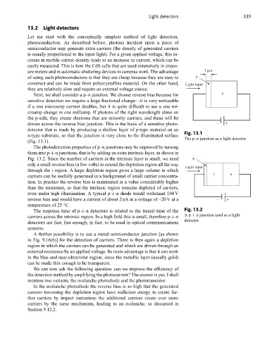
Next, we shall consider a p–n junction. We choose reverse bias because for n
sensitive detection we require a large fractional change—it is very noticeable
if a one microamp current doubles, but it is quite difficult to see a one mi-
croamp change in one milliamp. If photons of the right wavelength shine on
the p-side, they create electrons that are minority carriers, and these will be
driven across the reverse bias junction. This is the basis of a sensitive photo- – +
detector that is made by producing a shallow layer of p-type material on an
Fig. 13.1
n-type substrate, so that the junction is very close to the illuminated surface
The p–n junction as a light detector.
(Fig. 13.1).
The photodetection properties of p–n junctions may be improved by turning
them into p–i–n junctions, that is by adding an extra intrinsic layer, as shown in
Fig. 13.2. Since the number of carriers in the intrinsic layer is small, we need p
only a small reverse bias (a few volts) to extend the depletion region all the way
Light input
through the i region. A large depletion region gives a large volume in which
i n
carriers can be usefully generated in a background of small carrier concentra-
tion. In practice the reverse bias is maintained at a value considerably higher
than the minimum, so that the intrinsic region remains depleted of carriers,
even under high illumination. A typical p–i–n diode would withstand 100 V
reverse bias and would have a current of about 2 nA at a voltage of –20 V at a – +
◦
temperature of 25 C.
The response time of p–i–n detectors is related to the transit time of the Fig. 13.2
A p–i–n junction used as a light
carriers across the intrinsic region. In a high field this is small, therefore p–i–n
detector.
detectors are fast; fast enough, in fact, to be used in optical communications
systems.
A further possibility is to use a metal–semiconductor junction [as shown
in Fig. 9.16(b)] for the detection of carriers. There is then again a depletion
region in which the carriers can be generated and which are driven through an
external resistance by an applied voltage. Its main advantage is that it can work
in the blue and near-ultraviolet region, since the metallic layer (usually gold)
can be made thin enough to be transparent.
We can now ask the following question: can we improve the efficiency of
the detection method by amplifying the photocurrent? The answer is yes. I shall
mention two variants, the avalanche photodiode and the phototransistor.
In the avalanche photodiode the reverse bias is so high that the generated
carriers traversing the depletion region have sufficient energy to create fur-
ther carriers by impact ionization; the additional carriers create ever more
carriers by the same mechanism, leading to an avalanche, as discussed in
Section 9.12.2.