
Page 358 - Electrical Properties of Materials
P. 358
340 Optoelectronics
In a phototransistor the base is not connected. Instead, it is exposed to the
input light, which creates the carriers providing the base current. The base
current is then amplified in the usual manner.
Perhaps I should add that amplification is a good thing but not the only
thing to consider. Under certain conditions noise performance may be a more
important criterion when choosing a particular detector.
All the photodetectors mentioned so far needed an applied voltage. It should
be noted, however, that it is not necessary in this case. Light may be detected
in a p–n junction simply by short-circuiting it via a microammeter of very
low resistance, which serves as the load. The electrons and holes generated
by light in the junction will move under the effect of the built-in voltage and
drive a current through the ammeter. The measured current turns out to be
proportional to the input light intensity. This arrangement is usually referred
to as the photovoltaic operation of the junction.
A photovoltaic cell energized by the sun becomes a solar battery. When we
used to worry about the ‘energy crisis’ it was hoped that acres of solar cells
would replace nasty, dirty power stations. This has not quite come off, mainly
for economic reasons. A simple calculation shows that, even with a generous
estimate for the lifetime of a solar cell, the total energy it will generate is less
than that required to purify and fabricate the single crystal slice from which
it is made. So single crystals are definitely out, except for applications when
money is no object—as in space vehicles. Amorphous materials, however,
which we briefly discussed in Section 8.9, can be used, as the economics
are more favourable. The amorphous semiconductor with the most advanced
technology is silicon. It is possible to process it in a wide variety of ways,
so that its texture absorbs light well, and the actual absorption edge can be
shifted to give a better match to the sun’s output than is obtained by the much
more clearly defined single crystal. Amorphous silicon is usually deposited
in a vacuum or reduced gas pressure as a thin film. This makes it possible to
optimize the film thickness—thick enough to absorb light, but not so massive
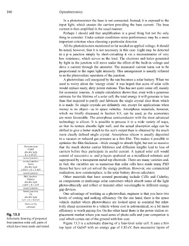
First junction that the much shorter carrier lifetimes and diffusion lengths lead to loss of
GaInP
absorbs light carriers before they participate in useful current. A typical solar cell would
E > 1.85 eV consist of successive n- and p-layers sputtered on a metallized substrate and
tunnel junction
second junction superposed by a transparent metal top electrode. There are many varieties and,
GaAs in fact, the variables are so numerous that solar cells have made many PhD
absorbs light
1.85eV > E > 1.4eV theses but have not yet solved the energy problem. However, one commercial
tunnel junction realization, now commonplace, is the solar battery driven calculator.
third junction Other materials that have seemed promising include CdTe and CuInSe 2
GaInAs
absorbs light as components in multistage solar converters which absorb some of the light
1.4eV > E > 1eV photovoltaically and reflect or transmit other wavelengths to different energy
tunnel junction gap devices.
fourth junction
Ge One advantage of working as a photovoltaic engineer is that you have two
absorbs light levels of costing and seeking efficiency. On the one hand, there is the space
1eV > E > 0.67eV
vehicle market where photovoltaics are looked upon as essential but relat-
GaAs or Ge
substrate ively cheap accessories to a vehicle whose cost is astronomical, so a bit more
efficiency is worth paying for. On the other hand there is the power station re-
Fig. 13.3 placement market where you need acres of photo cells and your competitor is
Schematic drawing of proposed coal which comes out of the ground with low cost.
four-junction solar cell, parts of Figure 13.3 is a schematic drawing of a four-level solar cell. It uses a thin
which have been made and tested.
top layer of GaInP with an energy gap of 1.85 eV, then successive layers of