
Page 361 - Electrical Properties of Materials
P. 361
Light emitting diodes (LEDs) 343
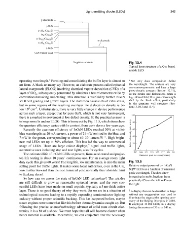
p-electrode
p-GaN
Ga N
p-Al 0.3 0.7
In Ga N
0.2
0.8
Ga N
n-In 0.02 0.98 n-electrode
n-Al Ga N
0.7
0.3
n-GaN
GaN buffer layer
Sapphire substrate Fig. 13.4
Typical layer structure of a QW based
nitride LED.
∗
operating wavelength. Forming and consolidating the buffer layer is almost an ∗ Not only does composition define
art form. A black art many say. However, an elaborate process called epitaxial the wavelength. The nitrides are very
lateral overgrowth (ELOG) involving chemical vapour deposition (CVD) of a non-centro-symmetric and have a large
piezo-electric constant (Section 10.11),
layerofSiO 2 , subsequently penetrated by windows a few micrometres wide by so the strains and dislocations cause a
conventional masking and etching. This structure is overlaid by further InGaN big internal field; this gives wavelength
MOCVD grading and growth layers. The distortion causes lots of extra strain, shift by the Stark effect, particularly
in the quantum well structure (Sec-
but in some regions of the resulting overlayer the dislocation density is be- tion 13.10.3 and 13.4).
–2
6
low 10 cm . Unfortunately, there is very little change in device performance
across such a layer, except that for pure GaN, which is not very luminescent,
100
there is a marked improvement at low defect density. So the practical answer is
to keep some In and no ELOG. This is borne out by Fig. 13.5, which shows how 80
the quantum efficiency varies with In content, from work done a few years ago.
Recently the quantum efficiency of InGaN LEDs reached 30% at violet- 60
blue wavelengths at 20 mA current, a power of 21 mW emitted in the blue, and Relative intensity (arb. units)
–1
7 mW in the green, corresponding to about 60–30 lumens W . High bright- 40
ness red LEDs are up to 50% efficient. This has led the way to commercial 20
†
usage of LEDs. There are large colour displays, signal and traffic lights,
automotive uses including stop and rear lights, also for cycles. 0
367 369 371 373 375 377 379 381
The estimated life of InGaN LEDs at present, from accelerated and projec- Emission peak wavelength (nm)
ted life testing is about 10 years’ continuous use. For an average room light
duty cycle this gives 60 years! The long life, low maintenance, is also the main Fig. 13.5
selling point for traffic lights. It makes some local authorities, even in the UK, Relative output power of uv InGaN
look further forward than the next financial year, normally their absolute limit SQW LEDs as a function of emission
peak wavelength. The dots show
to thinking ahead.
increasing In mole fractions from
So how can we assess the state of InGaN LED technology? The nitrides
practically 0% on the left to 4% on
are still difficult to grow as reasonable epitaxial layers, and the very suc-
the right.
cessful LEDs have been made on small crystals, typically a 5 nm-thick active
layer. There is no good theory of why they work. So we are in a situation of † A display that can be described as large
technological success leading to a rapidly expanding semiconductor lighting without any exaggeration was used to
industry without proper scientific backing. This has happened before, maybe illuminate the stage at the opening cere-
mony of the Beijing Olympics in 2008.
steam engines were somewhat like this before thermodynamics caught up. But It employed 44 000 LEDs in a display
following the precise science/technology advance of solid state circuit elec- having dimensions of 36 m × 147 m.
tronics, it is a bit of a shock. We must hope that all will become clearer when
better material is available. Meanwhile, we can conjecture that the necessary