
Page 366 - Electrical Properties of Materials
P. 366
348 Optoelectronics
(a) I
0 y
(b) N e
0 y
(c) N + D
0 y
(d) I
N +
D N e
0 y
(e) net charge density
0 y
(f) E
0 y
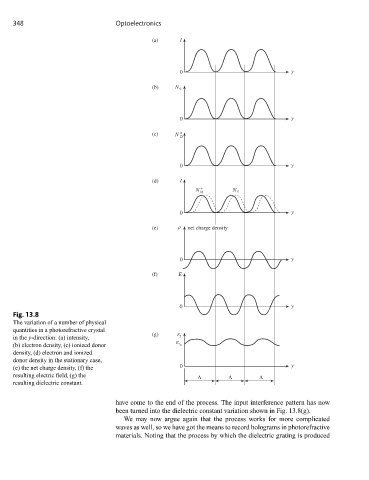
Fig. 13.8
The variation of a number of physical
quantities in a photorefractive crystal
in the y-direction: (a) intensity, (g) ε r
(b) electron density, (c) ionized donor ε r O
density, (d) electron and ionized
donor density in the stationary case,
(e) the net charge density, (f) the 0 y
resulting electric field, (g) the Λ Λ Λ
resulting dielectric constant.
have come to the end of the process. The input interference pattern has now
been turned into the dielectric constant variation shown in Fig. 13.8(g).
We may now argue again that the process works for more complicated
waves as well, so we have got the means to record holograms in photorefractive
materials. Noting that the process by which the dielectric grating is produced