Page 360 - Electrical Properties of Materials
P. 360
342                           Optoelectronics

                                   GaAlAs has been used to get well into the visible. These energy gaps are shown
                                   in Fig. 12.15 which also shows that the lattice parameters of GaAs and AlAs
     ∗  Electronegative atoms
                                   are very similar, so AlAs layers can be grown on GaAs substrate. LEDs in the
     When a covalent bond is formed between  blue and green were intially made from ZnS and ZnSe, using MBE, or even
     two different elements such as the III–Vs  ion implantation, to get both n- and p-types.
     or II–VIs, the electron distribution is not
     symmetrical between the elements be-  But the whole scenario of applications and usefulness of LEDs has changed
     cause it is energetically favourable for  in the past decade by the advent of InGaN devices. The nitrides were regarded
     the electron pair to be found closer to  by most people making LEDs in 1990 as ‘scientifically interesting’, which
     one atom. The atom which draws the  to commercially minded scientists, meant ‘black hole for time and money’.
     bonding electrons more closely to it is
     called more electronegative. This is a  However, the basic idea was attractive; if alloys of InN, GaN, and AlN were
     polar bond, in other words the covalent  available, LEDs could be made from direct gap semiconductors from the red
     bond is partly ionic, as we have shown  (1.89 eV) into the UV (6.2 eV). The main problem had been that there was no
     for some cases in Table 8.3. The follow-  way of getting a suitable substrate that could be used for epitaxial growth. The
     ing table was compiled by Linus Pauling
     (Table 13.1).                 nitrides, typically GaN, have the wurtzite structure, with strong ionicity due to
                                                               ∗
                                   the small, electronegative N atoms. So, the ionic as well as covalent nature
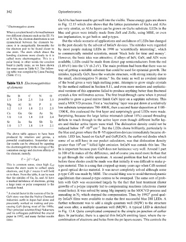
     Table 13.1 Electronegativities  of the bond gives a very high melting point. Attempts to grow single crystals
     of elements                   by the method outlined in Section 8.11, and even more modern and sophistic-
                                   ated versions of this apparatus failed to produce anything better than fractured
                                   crystals a few millimetres across. The first breakthrough came when it proved
     Be    B      C     N     O
     1.5   2.0    2.5   3.0   3.5  possible to grow a good mirror finish GaN layer on a sapphire substrate. This
                                   used a MOCVD process. First a ‘nucleating’ layer was put down at a relatively
     Mg    Al     Si    P     S
     1.2   1.5    1.8   2.1   2.5  low substrate temperature 700–800 K, then a second faster deposition at 1100–
                                   1300 K, this coalesced the first layer and surprisingly good LEDs were made.
     Ca    Ga     Ge    As    Se
     1.0   1.6    1.8   2.0   2.4  Surprising, because the large lattice mismatch (about 16%) caused threading
                                   defects to reach through to the active layer even though different buffer lay-
     Sr    In     Sn    Sb    Te
     1.0   1.7    1.8   1.9   2.1  ers and thicker active layers were tried. The dislocation density could not be
                                                 8
                                                     10
                                                         –2
                                   reduced below 10 –10 cm . But the LEDs shone brilliantly, particularly in
                                   the blue and green where the II–VI opposition devices immediately became ob-
     The above table appears to have been
     produced by intuition and genius, a  solete. LED law, based on GaAsP and GaP(ZnO), the earlier red diodes which
     powerful combination. Somewhat sim-  some of us still have in our pocket calculators, was that dislocation density
     ilar results can be obtained by equating  greater than 10 cm –2  killed light emission. InGaN was outside this law. The
                                               4
     the electronegativity to the average of the
     ionization energy and electron affinity of  In is important because pure GaN does not luminesce very well. Around 1 part
     the element, namely,          in 100 of In makes all the difference, and of course you need more In than that
                                   to get through the visible spectrum. A second problem that had to be solved
                1
             E = (I + E aff ).
                2                  before these diodes could be made was that initially it was difficult to make p-
                                   type material. This is a snag that cropped up many years ago when CdS seemed
     This is common sense, since high E aff
     means the atom wants to collect spare
     electrons, and high I means it will hold  a good optical device material. It was never completely solved although some
     on to them. From the table, it can be seen  p-type CdS was made by MBE. The crucial thing was to avoid thermodynamic
     that the nitrides of Ga, In, and Al have  equilibrium that caused p-type centres to be swamped. The same sort of prob-
     a marked imbalance of electrons, giving  lem with GaN was occasioned largely by the fact that heat treatment (faster
     a large ionic or polar component to the
     covalent bond.                growth) of a p-type impurity led to compensating reactions (electrons cluster
                                   round holes). It was solved by using Mg impurity in the MOCVD process and
     †  A crucial factor in the success of the In-                                     †
     GaN story was that the Nichia Chemical  annealing in N 2 which stopped the compensation. Thus, by 1992 good qual-
     Industries outfit in Japan had alone and  ity InGaN films were available to make the first successful blue DH LEDs. A
     presciently worked on making and pro-  further refinement was to add a single quantum well (SQW) to the structure
     cessing GaN during most of the 1980s.  and soon after, a multiple quantum well (MQW). A typical LED is sketched
     Their principal scientist Shuji Nakamura  in Fig. 13.4. Quite complicated compared to the simple pn junction of earlier
     and his colleagues published the crucial
     paper in 1992, and many further results  days. In particular, there is a special thin InGaN emitting layer, where the re-
     since.                        combination of electrons and holes from the pn layers occurs. This controls the

