
Page 284 - Embedded Microprocessor Systems Real World Design
P. 284
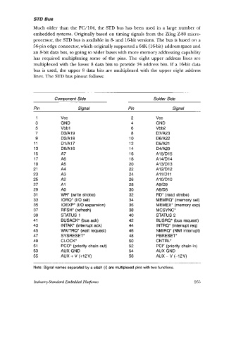
STD Bus

               Much older than the PC/104,  the STD bus has been used in a large number of
               embedded systems. Originally based on timing signals from the Zilog 2-80 micro-
               processor, the STD bus is available in 8- and 16-bit versions. The bus is based on a
               56-pin edge connector, which originally supported a 64K (16-bit) address space and
               an %bit data bus, so going to wider buses with more memory addressing capability
               has required  multiplexing  some of  the  pins. The eight upper  address lines are
               multiplexed with the lower 8 data bits to provide 24 address bits. If a  16-bit data
               bus is used, the upper  8 data bits are multiplexed with  the upper  eight address
               lines. The STD bus pinout follows:


                        Component Side                             Solder Side
               Pin                Signal                Pin                Signal

                1          vcc                           2          vcc
                3          GND                           4          GND
                5          Vbbl                          6          Vbb2
                7          D3/A 1 9                      8          D7lA23
                9          D2/A18                       10          D6lA22
                11         DllA17                       12          D5IA2 1
               13          DOlA16                       14          D4IA20
               15          A7                           16          A1 5/01 5
                17         A6                           18          A1 4ID14
               19          A5                           20          A13ID13
               21          A4                           22          A12/D12
               23          A3                           24          A1 1 ID 1 1
               25          A2                           26          A1  O/D 1 0
               27          A1                           28          A9ID9
               29          A0                           30          A8ID8
               31          WR* (write strobe)           32          RD+ (read strobe)
               33          IORQ'  (110 sel)             34          MEMRW (memory sel)
               35          IOEXP* (110 expansion)       36          MEMEX* (memory exp)
               37          RFSH" (refresh)              38          MCSYNC*
               39          STATUS 1                     40          STATUS 2
               41          BUSACK* (bus ack)            42          BUSRQ* (bus request)
               43          I NTAK+ (interrupt ack)      44          INTRW (interrupt req)
               45          WAITRW (wait request)        46          NMIRW (NMI interrupt)
               47          SYSRESET*                    48          PBRESET'
               49          CLOCK+                       50          CNTRL*
               51          PCO'  (priority chain out)   52          PCI* (priority chain in)
               53          AUX GND                      54          AUX GND
               55          AUX + V (+12V)               56          AUX - V  (-12V)

               Note: Signal names separated by a slash (/) are multiplexed pins with two functions.


               Industry-Standard Embedded Platjii                                   265