Page 204 - Engineering Digital Design
P. 204
4.9 FACTORIZATION, RESUBSTITUTION, AND DECOMPOSITION METHODS         175


                 gate path delay excluding possible inverters. The logic circuits considered to this point are
                 classified as two-level.


                 4.9.1 Factorization
                 The method of factorization is illustrated by using a simple example. Consider the minimum
                 SOP function
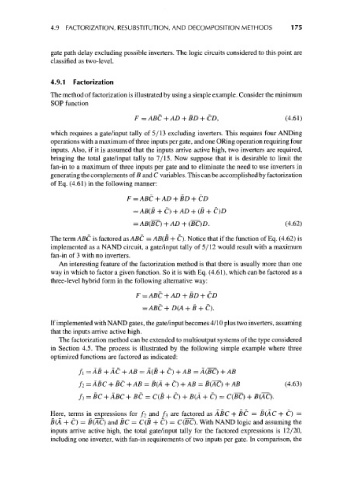
                                         F = ABC + AD + BD + CD,                    (4.61)

                 which requires a gate/input tally of 5/13 excluding inverters. This requires four ANDing
                 operations with a maximum of three inputs per gate, and one ORing operation requiring four
                 inputs. Also, if it is assumed that the inputs arrive active high, two inverters are required,
                 bringing the total gate/input tally to 7/15. Now suppose that it is desirable to limit the
                 fan-in to a maximum of three inputs per gate and to eliminate the need to use inverters in
                 generating the complements of B and C variables. This can be accomplished by factorization
                 of Eq. (4.61) in the following manner:
                                       F = ABC + AD + BD + CD

                                         = AB(B + C) + AD + (B + C}D
                                         = AB(BC) +AD + (BC)D.                       (4.62)

                 The term ABC is factored as ABC = AB(B + C). Notice that if the function of Eq. (4.62) is
                 implemented as a NAND circuit, a gate/input tally of 5/12 would result with a maximum
                 fan-in of 3 with no inverters.
                    An interesting feature of the factorization method is that there is usually more than one
                 way in which to factor a given function. So it is with Eq. (4.61), which can be factored as a
                 three-level hybrid form in the following alternative way:

                                          F = ABC + AD + BD + CD


                 If implemented with NAND gates, the gate/input becomes 4/10 plus two inverters, assuming
                 that the inputs arrive active high.
                    The factorization method can be extended to multioutput systems of the type considered
                 in Section 4.5. The process is illustrated by the following simple example where three
                 optimized functions are factored as indicated:
                         fi = A

                         / 2 = ABC + BC+AB = B(A + C)+AB = B(AC) + AB               (4.63)
                         / 3 = BC + ABC + BC = C(B + C) + B(A + C) = C(BC) + B(AC).

                 Here, terms in expressions for /2 and /3 are factored as ABC + BC = B(AC + C) =
                 B(A + C) = B(AC) and BC = C(B + C) = C(BC). With NAND logic and assuming the
                 inputs arrive active high, the total gate/input tally for the factored expressions is 12/20,
                 including one inverter, with fan-in requirements of two inputs per gate. In comparison, the

