
Page 209 - Engineering Digital Design
P. 209
180 CHAPTER 4 /LOGIC FUNCTION REPRESENTATION AND MINIMIZATION
functions of a large number of variables by using devices with lesser input capability. The
use of multiplexers discussed in Section 6.2 offers a good example of this fact.
The process of decomposition can be reversed to yield a purely SOP or purely POS
expression from the decomposed expression. This is illustrated by factoring out A, A, B,
and B in turn from F AB to yield the SOP expression
F AB = AB(D) + A B(C) + AB(C 0 £>) + AB(C + D)
= A [BD + BC] + A[B(C 0 D) + B(C + D)]
= AB[D]+AB[C] +AB[CD + CD] + AB[C + D]
= ABD+ABC+ABCD
where C © D = CD + CD follows from Eq. (3.4). A cursory inspection of the SOP form
of F AB verifies its agreement with Fig. 4.48.
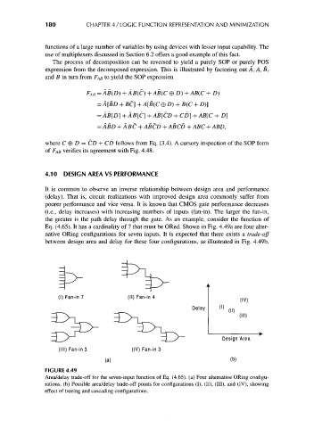
4.10 DESIGN AREA VS PERFORMANCE
It is common to observe an inverse relationship between design area and performance
(delay). That is, circuit realizations with improved design area commonly suffer from
poorer performance and vice versa. It is known that CMOS gate performance decreases
(i.e., delay increases) with increasing numbers of inputs (fan-in). The larger the fan-in,
the greater is the path delay through the gate. As an example, consider the function of
Eq. (4.65). It has a cardinality of 7 that must be ORed. Shown in Fig. 4.49a are four alter-
native ORing configurations for seven inputs. It is expected that there exists a trade-off
between design area and delay for these four configurations, as illustrated in Fig. 4.49b.
(I) Fan-in 7 (II) Fan-in 4
(IV)
Delay (I)
(II)
Design Area
(III) Fan-in 3 (IV) Fan-in 3
(a) (b)
FIGURE 4.49
Area/delay trade-off for the seven-input function of Eq. (4.65). (a) Four alternative ORing configu-
rations, (b) Possible area/delay trade-off points for configurations (I), (II), (III), and (IV), showing
effect of treeing and cascading configurations.