
Page 136 - Environmental Nanotechnology Applications and Impacts of Nanomaterials
P. 136
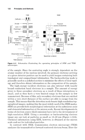
122   Principles and Methods


                         TEM                          SEM
               Cathode

               Anode                               source of electrons
                                                      Filament
           Condensor  Diaphragm                     Anode   Image
               Lens
               Lens
                                                     Condenser     Scan
                                                                 generator
                  Specimen
          Condensor  aperture  Diaphragm  Beam      Magnification
                                   EDS
                Lens
             Intermediary
               lens                                     control  Cathode
                                                      objective
                                                     Photo multiplier
            Observation screen
                                          Specimen collector
              TEM detector
        Figure 4.11  Schematics illustrating the operating principles of SEM and TEM
        microscopes.

        of the sample. Since the scattering angle is strongly dependent on the
        atomic number of the nucleus involved, the primary electrons arriving
        at a given detector position can be used to yield images containing both
        topological and compositional information. The backscattering mode is
        generally used on a polished section to minimize the effects of local topol-
        ogy and therefore obtain information on the composition of the sample.
          The high-energy incident electrons can also interact with loosely
        bound conduction band electrons in a sample. The amount of energy
        given to these secondary electrons as a result of these interactions is
        small, and so they have a very limited range in the sample (a few
        nanometers). Because of this, only secondary electrons that are emitted
        within a very short distance of the surface are able to escape from the
        sample. This means that the detection mode boasts high-resolution top-
        ographical images, making this the most widely used of the SEM modes.
        SEM can provide both morphological information at the submicron scale
        and elemental information at the micron scale. Recent developments in
        terms of electron source (field emission) have led to the development of
        high-resolution SEM. Using a secondary or backscattering electron
        image one can look at particles as small as 10–20 nm (Figure 4.12A).
        Chemical information using EDX, however, is obtained at the micron
        scale and not for individual particles.
          In contrast with SEM, transmission electron microscopy (TEM)
        analyzes the transmitted or forward-scattered electron beam. Here the