
Page 137 - Environmental Nanotechnology Applications and Impacts of Nanomaterials
P. 137
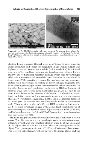
Methods for Structural and Chemical Characterization of Nanomaterials  123


        Figure 4.12  A. An FESEM secondary electron image of Ag nanoparticles where the
        particle size is determined using the appropriate scale (courtesy of Vladimir Tarabara).
        B. A TEM image of imogolite (single-walled aluminosilicate nanotube) (courtesy of
        Clément Levard).


        electron beam is passed through a series of lenses to determine the
        image resolution and obtain the magnified image (Figure 4.12B). The
        highest structural resolution possible (point resolution) is achieved
        upon use of high-voltage instruments (acceleration voltages higher
        than 0.5 MeV). Enhanced radiation damage, which may have stronger
        effects for nanostructured materials, must however be considered in
        these cases. With corrections it is possible to achieve sub-angstrom res-
        olution with microscopes operating at lower voltages (typically, 200
        keV), allowing the oxygen atoms to be resolved in oxides materials. On
        the other hand, as high resolution is achieved in TEM as the result of
        electron wave interference among diffracted peaks and not only to the
        transmitted beam in the absence of deflection, a limitation to struc-
        tural resolution can arise from nanoparticles with a very low number
        of atoms. Nevertheless conventional TEM is the most common tool used
        to investigate the crystal structure of materials at the sub-nanometer
        scale. There exist a number of different TEM techniques that may be
        used to obtain structural images with atomic level resolution; two of
        these techniques are detailed below: high-resolution TEM (HRTEM)
        and high angle annular dark field (HAADF) scanning transmission elec-
        tron microscopy (STEM).
          HRTEM images are formed by the interference of coherent electron
        waves. The object transmits the (nearly) planar incident electron wave,
                                                          at the exit plane
        interacts with it, and the resulting electron wave   e
        of the object carries information about the atom arrangement in the
        object. The   corresponds to a set of “diffracted” coherent plane waves.
                    e
        The electron optics transfers these waves to the image plane, and the