
Page 292 - Fundamentals of The Finite Element Method for Heat and Fluid Flow
P. 292
SOME EXAMPLES OF FLUID FLOW AND HEAT TRANSFER PROBLEMS
284
the chip (location of the maximum temperature) and the ambient, referred to as R ja and
defined as
T j − T a
R ja = (9.1)
P
where T j is the chip temperature, T a is the ambient temperature and P is the power
dissipated by the chip.
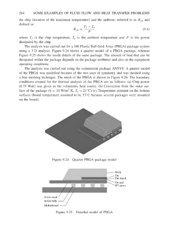
The analysis was carried out for a 106 Plastic Ball Grid Array (PBGA) package system
using a 3-D analysis. Figure 9.24 shows a quarter model of a PBGA package, whereas
Figure 9.25 shows the inside details of the same package. The amount of heat that can be
dissipated within the package depends on the package attributes and also on the equipment
operating conditions.
The analysis was carried out using the commercial package ANSYS. A quarter model
of the PBGA was modelled because of the two axes of symmetry and was meshed using
a free meshing technique. The mesh of the PBGA is shown in Figure 9.26. The boundary
conditions created for the thermal analysis of the PBGA are as follows: (a) Chip power
(0.75 Watt) was given as the volumetric heat source. (b) Convection from the outer sur-
2
face of the package (h = 10 W/m K, T a = 21 C) (c) Temperature restraint on the bottom
◦
surfaces (board temperature assumed to be 53 C because several packages were mounted
◦
on the board).
Figure 9.24 Quarter PBGA package model
Mold
Die
Die attach
Die pad
BT epoxy
Solder mask
Solder balls
Motherboard
Figure 9.25 Detailed model of PBGA