
Page 156 - Introduction to Colloid and Surface Chemistry
P. 156
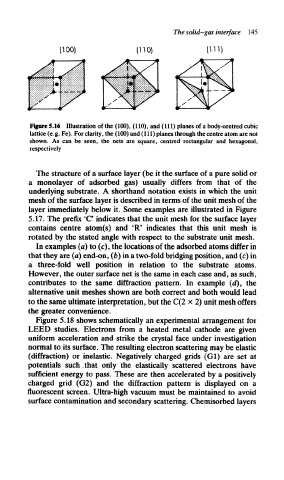
The solid-gas interface  145
                                                       (111)
                 (100)               (110)


         Figure 5.16  Illustration of the  (100), (110), and  (111)  planes of a body-centred cubic
         lattice (e.g.  Fe).  For clarity, the (100) and (111) planes through the centre atom are not
         shown.  As  can  be  seen,  the  nets  are  square,  centred  rectangular  and  hexagonal,
         respectively


          The structure of a surface layer (be it the surface of a pure solid or
        a  monolayer  of  adsorbed  gas)  usually  differs  from  that  of  the
         underlying substrate.  A  shorthand  notation  exists  in which  the unit
         mesh of the  surface layer is described  in terms of the unit mesh of the
         layer immediately below it.  Some  examples  are  illustrated in  Figure
        5.17.  The prefix 'C' indicates that the unit mesh for the surface layer
        contains  centre  atom(s)  and  'R'  indicates  that  this  unit  mesh  is
        rotated  by the  stated  angle  with  respect  to  the  substrate  unit  mesh.
          In examples (a) to (c), the locations  of the adsorbed  atoms differ in
        that they are (a) end-on,  (b) in a two-fold bridging position, and (c) in
        a  three-fold  well  position  in  relation  to  the  substrate  atoms.
        However,  the outer surface net is the same in each case and, as such,
        contributes  to  the  same  diffraction  pattern.  In  example  (</),  the
        alternative  unit meshes  shown are both correct  and both would lead
        to the same ultimate interpretation, but the C(2 x  2) unit mesh  offers
        the greater  convenience.
          Figure  5.18  shows schematically an experimental arrangement for
        LEED   studies.  Electrons  from  a  heated  metal  cathode  are  given
        uniform  acceleration  and  strike  the  crystal face  under  investigation
        normal to its surface. The resulting electron  scattering  may be  elastic
        (diffraction)  or  inelastic.  Negatively -charged  grids  (Gl)  are  set  at
        potentials  such .that  only  the  elastically  scattered  electrons  have
        sufficient  energy  to  pass.  These  are then accelerated  by a positively
        charged  grid  (G2)  and  the  diffraction  pattern  is  displayed  on  a
        fluorescent  screen.  Ultra-high  vacuum must be  maintained  to  avoid
        surface  contamination and secondary scattering. Chemisorbed layers