
Page 498 - Introduction to Information Optics
P. 498
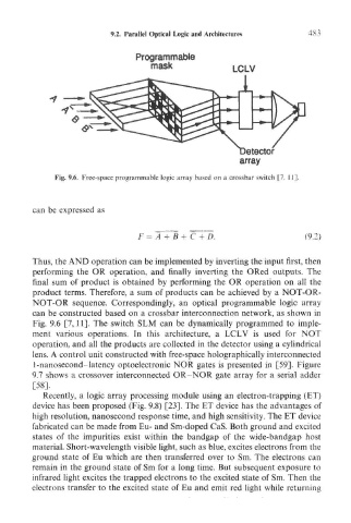
9.2. Parallel Optical Logic and Architectures


                                                         elector
                                                       array

            Fig. 9.6. Free-space programmable logic array based on a crossbar switch [7. 11].


       can be expressed as

                                                                      (9,2)


       Thus, the AND operation can be implemented by inverting the input first, then
       performing the OR operation, and finally inverting the ORed outputs. The
       final sum of product is obtained by performing the OR operation on all the
       product terms. Therefore, a sum of products can be achieved by a NOT-OR-
       NOT-OR sequence. Correspondingly, an optical programmable logic array
       can be constructed based on a crossbar interconnection network, as shown in
       Fig. 9.6 [7,11]. The switch SLM can be dynamically programmed to imple-
       ment various operations. In this architecture, a LCLV is used for NOT
       operation, and all the products are collected in the detector using a cylindrical
       lens. A control unit constructed with free-space holographically interconnected
       1-nanosecond-latency optoelectronic NOR gates is presented in [59]. Figure
       9.7 shows a crossover interconnected OR-NOR gate array for a serial adder
       [58].
          Recently, a logic array processing module using an electron-trapping (ET)
       device has been proposed (Fig. 9.8) [23]. The ET device has the advantages of
       high resolution, nanosecond response time, and high sensitivity. The ET device
       fabricated can be made from Eu- and Sm-doped CaS. Both ground and excited
       states of the impurities exist within the bandgap of the wide-bandgap host
       material. Short-wavelength visible light, such as blue, excites electrons from the
       ground state of Eu which are then transferred over to Sm. The electrons can
       remain in the ground state of Sm for a long time. But subsequent exposure to
       infrared light excites the trapped electrons to the excited state of Sm. Then the
       electrons transfer to the excited state of Eu and emit red light while returning