
Page 43 - Introduction to Microcontrollers Architecture, Programming, and Interfacing of The Motorola 68HC12
P. 43
20 Chapter 1 Basic Computer Structure and the 6812
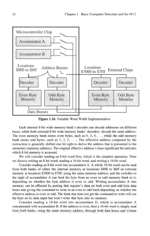
Figure 1.16. Variable Word Width Implementation
Each internal 8-bit wide memory bank's decoder can decode addresses on different
buses, while both external 8-bit wide memory banks' decoders decode the same address.
The even memory bank stores even bytes, such as 0, 2, 4, . . . while the odd memory
bank stores odd bytes, such as 1, 3, 5, .... The effective address computed by the
instruction is generally shifted one bit right to derive the address that is presented to the
memories (memory address). The original effective address's least significant bit indicates
which 8-bit memory is accessed.
We will consider reading an 8-bit word first, which is the simplest operation. Then
we discuss writing an 8-bit word, reading a 16-bit word, and writing a 16-bit word.
Consider reading an 8-bit word into accumulator A. A whole 16-bit word can be read
from both banks of either the internal memory at locations $800 to $bff or external
memory at locations $7000 to $7fff, using the same memory address; and the switches to
the right of accumulator A can feed the byte from an even or odd memory bank to it,
depending on whether the byte address is even or odd. Writing accumulator A into
memory can be effected by putting that register's data on both even and odd byte data
buses and giving the command to write to an even or odd bank depending on whether the
effective address is even or odd. The bank that does not get the command to write will see
the byte on its data input but won't write that byte into its memory.
Consider reading a 16-bit word into accumulator D, which is accumulator A
concatenated with accumulator B. If the address is even, then a 16-bit word is simply read
from both banks, using the same memory address, through both data buses and written