
Page 292 - System on Package_ Miniaturization of the Entire System
P. 292
266 Cha pte r F i v e
Embedded organic
LCP | New polymers
MEMS BAW GaAs RFCMOS Future
PICS (10X reduction in
Package integration 5 μm Lithography
X, Y, and Z)
1000
on Si wafer
2
components/cm
Embedded RF SOP
ceramic
ceramic, silicon 100 components/cm 2
IPD
Current
50 μm Lithography
Discrete
components
Past
Ceramic thick film
200 μm Lithography
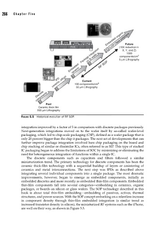
FIGURE 5.5 Historical evolution of RF SOP.
integration improved by a factor of 5 in comparison with discrete packages previously.
Next-generation integrations moved on to the wafer itself by so-called wafer-level
packaging, which led to chip-scale packaging (CSP), defined as a wafer package that is
only 20 percent bigger than the chip it packages. The next set of developments that can
further improve package integration involved bare chip packaging on the board and
chip stacking of similar or dissimilar ICs, often referred to as SIP. This type of stacked
IC packaging began to address the limitations of SOC by minimizing or eliminating the
need for heterogeneous integration of functions within a single IC.
The discrete components such as capacitors and filters followed a similar
miniaturization trend. The primary technology for discrete components has been the
ceramic thick-film technology with a sequential buildup of layers or cosintering of
ceramics and metal interconnections. The next step was IPDs as described above
integrating several individual components into a single package. The most dramatic
improvements, however, began to emerge as embedded components, initially as
embedded discretes and more recently as embedded thin-film components. Embedded
thin-film components fall into several categories—embedding in ceramics, organic
packages, or boards on silicon or glass wafers. The SOP technology described in this
book is about total thin-film embedding—embedding of passives, actives, thermal
structures, and power sources. With the SOP concept embarking on a relentless increase
in component density through thin-film embedded integration (a similar trend as
increased transistor density in silicon), the miniaturized RF systems such as the iPhone,
are well on their way, as shown in Figure 5.5.