
Page 336 - System on Package_ Miniaturization of the Entire System
P. 336
310 Cha pte r F i v e
5.5.2 Intelligent Network Communicator (INC)
A highly integrated mixed-signal testbed was developed to demonstrate the concept
and realization of the advanced system-on-package concept [6]. This experimental
system called Intelligent Network Communicator (INC) deals with three different
statuses of the signals (digital, RF, and optical) in a single packaging platform. The INC
transmits and receives the high-speed digital signal and wireless signal over the
embedded optical waveguide channel. The system has been fabricated by utilizing
advanced packaging and assembly processes, and full functionality has been
demonstrated successfully. Before the final test, each of the subblocks has been separately
developed and tested. The test results clearly show that the developed system
performance meets the goal. The digital block generated up to 3.2 Gbytes/s of data
stream, and the RF block has less than –1.5 dB of insertion loss up to 6 GHz. The optical
block achieved 10 Gbytes/s throughput over the embedded optical waveguide built on
the low-cost organic substrate.
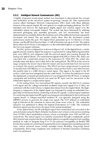
The INC system configuration is shown in Figure 5.45. At the digital block, a multi-
gigabit pseudo random digital bit sequence is generated by using field-programmable
gate array (FPGA) and compared with the received signal after passing through the
analog and optical blocks. The multichannel signals from FPGA (Virtex 50E, Xlinx) are
converted into a serial data stream by the transceiver IC (TLK 2701, TI), which also
includes mux and dmux and is then fed to the analog block. The FPGA at the receiver
stage compares the known input data bit stream and recovered data from the receiver
to evaluate the system performance. The FPGA has been programmed to generate
16 parallel data (150 Mbytes/s/c/s) channels, which are then fed to a mux that converts
the parallel data to a 2.488 Gbytes/s serial signal. This signal is the input to the RF
section, which has been integrated into the same board. To reduce the interference from
the digital part, a separate ground and power was designed for the RF block. A coplanar
waveguide and matching network was used for RF input and for conversion of the
differential signal to a single-ended signal.
At the analog block, two narrowband RF signals, namely, the 802.11a/b wireless
LAN signal and the voltage-controlled oscillator single tone signal (5 to 6 GHz), are
combined with the multi-Gbytes/s digital data stream from the digital block. The high-
frequency component of the digital signal was truncated by using an embedded low-
pass filter in the board, before combining with the RF signals. A mixed-signal combiner
for combining the digital and RF signal was designed and embedded in the multilayered
organic board. A voltage-controlled oscillator IC was specially designed using the
MESFET process to generate the single tone signal. The VCO utilized an embedded
high-Q inductor in the substrate to reduce the phase noise of the IC. The embedded
inductor was optimized to obtain the highest performance at 5 GHz. The combined
electrical signal was then fed to the input of the optical modulator.
At the optical block, the RF and digital signal were modulated and converted to the
optical domain using the Mach-Zehnder modulator and vertical-cavity surface-emitting
laser (VCSEL) direct modulation scheme, whose wavelengths were 1550 and 870 nm,
respectively. The optical signal was initially transmitted through a multimode optical
fiber channel and coupled into the embedded optical waveguide using the butt-coupling
method. In order to integrate long (5 to 15 cm) polymer waveguides on flexible FR4
boards that contain two metal layers separated by a low-temperature insulating polymer
layer, critical technical issues (which included board flexibility, long-range board
nonplanarity, short-range roughness and coefficient of thermal expansion matching)
had to be addressed.