
Page 337 - System on Package_ Miniaturization of the Entire System
P. 337
Radio Fr equency System-on-Package (RF SOP) 311
Digital block Analog block Optic block
Up-mixer
RF In
VCO Laser coiler
FPGA .... MUX D.S
Power combiner
Driver Amp
Multiple Down-mixer
differential RF Out Embedded optical detector
channel
VCO
FPGA .... DMUX S.D TIA Embedded
photo
Power doubler
detector
(a)
(b)
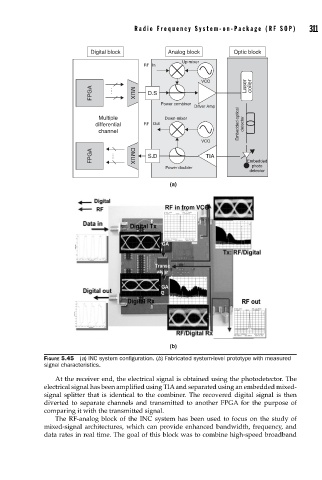
FIGURE 5.45 (a) INC system confi guration. (b) Fabricated system-level prototype with measured
signal characteristics.
At the receiver end, the electrical signal is obtained using the photodetector. The
electrical signal has been amplified using TIA and separated using an embedded mixed-
signal splitter that is identical to the combiner. The recovered digital signal is then
diverted to separate channels and transmitted to another FPGA for the purpose of
comparing it with the transmitted signal.
The RF-analog block of the INC system has been used to focus on the study of
mixed-signal architectures, which can provide enhanced bandwidth, frequency, and
data rates in real time. The goal of this block was to combine high-speed broadband