
Page 19 - MEMS Mechanical Sensors
P. 19
8 Materials and Fabrication Techniques
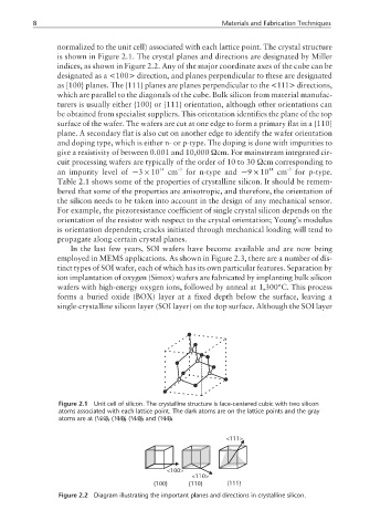
normalized to the unit cell) associated with each lattice point. The crystal structure
is shown in Figure 2.1. The crystal planes and directions are designated by Miller
indices, as shown in Figure 2.2. Any of the major coordinate axes of the cube can be
designated as a <100> direction, and planes perpendicular to these are designated
as {100} planes. The {111} planes are planes perpendicular to the <111> directions,
which are parallel to the diagonals of the cube. Bulk silicon from material manufac-
turers is usually either {100} or {111} orientation, although other orientations can
be obtained from specialist suppliers. This orientation identifies the plane of the top
surface of the wafer. The wafers are cut at one edge to form a primary flat in a {110}
plane. A secondary flat is also cut on another edge to identify the wafer orientation
and doping type, which is either n- or p-type. The doping is done with impurities to
give a resistivity of between 0.001 and 10,000 Ωcm. For mainstream integrated cir-
cuit processing wafers are typically of the order of 10 to 30 Ωcm corresponding to
an impurity level of ∼3 × 10 14 cm –3 for n-type and ∼9 × 10 14 cm –3 for p-type.
Table 2.1 shows some of the properties of crystalline silicon. It should be remem-
bered that some of the properties are anisotropic, and therefore, the orientation of
the silicon needs to be taken into account in the design of any mechanical sensor.
For example, the piezoresistance coefficient of single crystal silicon depends on the
orientation of the resistor with respect to the crystal orientation; Young’s modulus
is orientation dependent; cracks initiated through mechanical loading will tend to
propagate along certain crystal planes.
In the last few years, SOI wafers have become available and are now being
employed in MEMS applications. As shown in Figure 2.3, there are a number of dis-
tinct types of SOI wafer, each of which has its own particular features. Separation by
ion implantation of oxygen (Simox) wafers are fabricated by implanting bulk silicon
wafers with high-energy oxygen ions, followed by anneal at 1,300°C. This process
forms a buried oxide (BOX) layer at a fixed depth below the surface, leaving a
single-crystalline silicon layer (SOI layer) on the top surface. Although the SOI layer
Figure 2.1 Unit cell of silicon. The crystalline structure is face-centered cubic with two silicon
atoms associated with each lattice point. The dark atoms are on the lattice points and the gray
atoms are at (¼ ¼ ¼), (¼ ¾ ¾), (¾ ¼ ¾), and (¾ ¾ ¼).
Figure 2.2 Diagram illustrating the important planes and directions in crystalline silicon.