
Page 20 - MEMS Mechanical Sensors
P. 20
2.2 Materials 9
Table 2.1 Selected Properties of Crystalline Silicon
9
–2
Yield strength (10 Nm ) 7
–2
Knoop hardness (kgmm ) 850
Young’s modulus (GPa), (100) orientation 160
Poisson’s ratio, (100) orientation 0.28
–3
Density (gcm ) 2.33
Lattice constant (Å) 5.435
–6
–1
Thermal expansion coefficient (10 K ) 2.6
–1
–1
Thermal conductivity (Wm K ) 157
–1
–1
Specific heat (Jg K ) 0.7
Melting point (°C) 1,410
Energy gap (eV) 1.12
Dielectric constant 11.9
–1
7
Dielectric strength (10 Vm ) 3
–1 –1
2
Electron mobility (cm V s ) 1,450
2
–1 –1
Hole mobility (cm V s ) 505
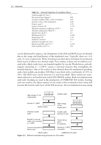
can be thickened by epitaxy, the thicknesses of the SOI and BOX layers are limited
due to the range and distribution of the implanted ions. Typically, these are ~0.2
and ∼0.1 µm, respectively. Wafer bonding is an alternative technique for producing
thick layers of silicon on a buried oxide. Two wafers, at least one of which is cov-
ered with a thick oxide layer, are bonded together by van der Waals forces, and sub-
sequent annealing at ∼1,100°C causes a chemical reaction that strengthens the
bonded interface. One of the wafers is then thinned down by mechanical grinding,
and a final polish can produce SOI films 1 µm thick with a uniformity of 10% to
30%. The BOX layer can be between 0.5 and 4 µm thick. These wafers are some-
times referred to as bonded and etched SOI (BESOI) wafers. Both ion implantation
and wafer bonding are used in the production of UNIBOND SOI wafers. Starting
with two wafers, the silicon surface of one wafer is first oxidized to form what will
become the buried oxide layer of the SOI structure. An ion implantation step, using
Oxidize wafer
+
High energy O ion
implantation
Anneal at 1,300ºC High energy
+
H ion
SIMOX wafers implantation
Oxidized handle Handle wafer
wafer bonded on top
Bonded to second Cleave along
wafter and annealed plane
at 1,100ºC
of weakness
Ground and polished Anneal at 1,100ºC
device layer and polish
BESOI wafers UNIBOND SOI wafers
Figure 2.3 Different manufacturing processes for SOI wafers.