
Page 25 - MEMS Mechanical Sensors
P. 25
14 Materials and Fabrication Techniques
2.3.1.4 Epitaxy
Epitaxial silicon can be grown by APCVD or LPCVD. The ranges of temperatures at
which this is done are 900°C to 1,250°C for APCVD and 700°C to 900°C for
LPCVD. Epitaxy can be used to deposit silicon layers with clearly defined doping
profiles that can be used as an etch stop, such as, for example, an electrochemical
etch stop. It can also be used to thicken the SOI layers on Simox or UNIBOND
wafers, for which the thickness of the original SOI layer is restricted by the manufac-
turing process. The most useful property of epitaxial silicon for MEMS applications,
though, may be the fact that it can be grown selectively. Silicon dioxide or silicon
nitride on wafers prevents the growth of epitaxial silicon, and a layer of amorphous
silicon or polysilicon is normally deposited instead. However, this deposition
process can be suppressed by the addition of HCl to the reaction gases. The HCl pre-
vents spurious nucleation and growth of silicon on the silicon dioxide or nitride. An
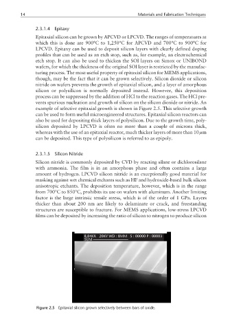
example of selective epitaxial growth is shown in Figure 2.5. This selective growth
can be used to form useful microengineered structures. Epitaxial silicon reactors can
also be used for depositing thick layers of polysilicon. Due to the growth time, poly-
silicon deposited by LPCVD is often no more than a couple of microns thick,
whereas with the use of an epitaxial reactor, much thicker layers of more than 10 µm
can be deposited. This type of polysilicon is referred to as epipoly.
2.3.1.5 Silicon Nitride
Silicon nitride is commonly deposited by CVD by reacting silane or dichlorosilane
with ammonia. The film is in an amorphous phase and often contains a large
amount of hydrogen. LPCVD silicon nitride is an exceptionally good material for
masking against wet chemical etchants such as HF and hydroxide-based bulk silicon
anisotropic etchants. The deposition temperature, however, which is in the range
from 700°C to 850°C, prohibits its use on wafers with aluminum. Another limiting
factor is the large intrinsic tensile stress, which is of the order of 1 GPa. Layers
thicker than about 200 nm are likely to delaminate or crack, and freestanding
structures are susceptible to fracture. For MEMS applications, low-stress LPCVD
films can be deposited by increasing the ratio of silicon to nitrogen to produce silicon
8,84KX 20KV WD : 8MM S : 00000 P : 00003
5UM
Figure 2.5 Epitaxial silicon grown selectively between bars of oxide.