
Page 30 - MEMS Mechanical Sensors
P. 30
2.3 Fabrication Techniques 19
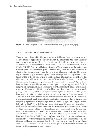
Figure 2.7 SEM photograph of microlens array fabricated using grayscale lithography.
2.3.2.3 Thick and Laminated Photoresists
There are a number of thick UV photoresists available and these have been used in a
diverse range of applications. In conventional IC processing, the resist thickness
spun on to the wafer is of the order of a micron thick, which means that 3 to 4 µm
and above should be regarded as a thick resist. There are some thick resists, such as
Shipley SPR 220-7, which will give a thickness of 7 µm if spun on to the wafer at the
manufacturer’s recommended speed. The thickness, however, can be increased by
slowing the spin speed, and thicker layers of up to 60 µm can be obtained by repeat-
ing the process to give multiple layers. Other resists give thicker layers still, some-
times of the order of 500 µm in a single coating. Maintaining control over the
thickness and uniformity becomes more difficult as the thickness increases. The
thick resist most frequently reported on is the photoplastic polymer SU-8, which has
been used as a micromold for injection molding or electroplating, as a mask for deep
reactive ion etching (DRIE), as a structural MEMS component, and as a mechanical
material. When cured, SU-8 forms a highly crosslinked matrix of covalent bonds
giving it a wide range of elastic properties without plastic deformation. Thus, it has
been used to make compliant structures such as springs and microgrippers [5].
There have been some reports on the difficulties associated with SU-8—for exam-
ple, stress induced crack generation in mechanical structures—but by far the most
frequently reported difficulty is the problem of removing it [6]. Both oxygen plasma
[7] and hot NMP (1-methyl-2-pyrrolidinone) stripper [8] have been used, but in
each case the removal has been either slow or incomplete. JSR manufactures a range
of thick photoresists, which, it is claimed, can easily be stripped using the manufac-
turers own photoresist stripper and acetone [8]. Thicknesses of 1.4 mm have been
reported for a double coating of JSR THB-430N. However, this resist has so far not
been widely used in MEMS. A dry film photoresist, Ordyl P-50100, has been used
successfully to form electroplating molds up to 100 µm thick, without any of the dif-
ficulties and limitations mentioned earlier [9]. An obstacle to using dry resists, how-
ever, is that application of the resist is done using a hot roll laminator, not normally
found in silicon processing clean-rooms.