
Page 26 - MEMS Mechanical Sensors
P. 26
2.3 Fabrication Techniques 15
rich nitride or by adding N O to the reaction gases, thereby depositing silicon
2
oxynitride. Silicon nitride deposited by PECVD contains substantially more hydro-
gen than LPCVD nitride and is nonstoichiometric. Deposition temperatures are
between 250°C and 350°C, thus making it possible to deposit it on wafers with
aluminum interconnects. Stress in the films is a function of pressure, temperature,
frequency, power, and gas composition and is in the range from –600 MPa (com-
pressive) to +600 MPa (tensile). Films deposited at 50 kHz and 300°C are compres-
sive, but at about 600°C the stress switches from compressive to tensile, making the
deposition of low stress films possible. Unfortunately, this eliminates one of the
advantages of PECVD, that is, low temperature deposition. Films deposited at
13.56 MHz are tensile and whereas most PECVD equipment operates at a fixed fre-
quency, some equipment manufacturers have enabled their systems to be switched
rapidly between high and low frequencies to obtain very low stress films. The step
coverage of PECVD silicon nitride is conformal; however, the pinhole density and
stress can be a problem if it is used as a masking material against wet chemical
etchants. The exact film properties vary depending on the system, the gas purity,
and the deposition conditions, yet, with the right conditions, low pinhole densities,
conformal step coverage, and low stress layers can be obtained. Some properties of
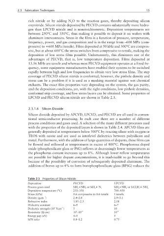
LPCVD and PECVD silicon nitride are shown in Table 2.3.
2.3.1.6 Silicon Dioxide
Silicon dioxide deposited by APCVD, LPCVD, and PECVD are all used in conven-
tional semiconductor processing. In each case there are a number of different
process conditions and gases used. A selection of the many different processes used
with the properties of the deposited layers is shown in Table 2.4. APCVD films are
generally deposited at temperatures below 500°C by reacting silane with oxygen or
TEOS with ozone and are used as interlevel dielectrics between polysilicon and
metal. Furthermore, with the addition of large quantities of dopants, these films can
be flowed and reflowed at temperatures in excess of 800°C. Phosphorous doped
oxide (phosphosilicate glass or PSG) reflows at decreasingly lower temperatures as
the phosphorus content increases up to 8%. Although lower reflow temperatures
are possible for higher dopant concentrations, it is inadvisable to go beyond this
because of the possibility of corrosion of subsequently deposited aluminum. The
addition of boron up to 4% to form borophosphosilicate glass (BPSG) reduces the
Table 2.3 Properties of Silicon Nitride
Deposition PECVD LPCVD
Process gases used SiH +NH or SiH + N SiH +NH or SiCl H + NH
4 4 4 2 4 4 2 2 4
Deposition temperature (°C) 250–350 700–850
Stress (GPa) 0.6 compressive to 0.6 tensile 1 tensile
−1
Density (gcm ) 2.4–2.8 2.9–3.1
Refractive index 1.85–2.5 2.01
Dielectric constant 6–9 6–7
6
−1
Dielectric strength (10 Vcm ) 5 10
6
Resistivity (Ω-cm) 10 –10 15 10 16
Energy gap (eV) 4–5 5
Si/N ratio 0.8–1.2 0.75