
Page 23 - MEMS Mechanical Sensors
P. 23
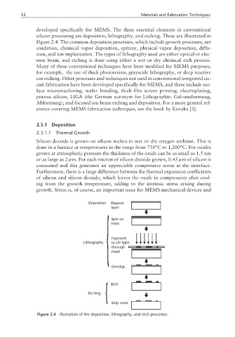
12                                                 Materials and Fabrication Techniques

                 developed specifically for MEMS. The three essential elements in conventional
                 silicon processing are deposition, lithography, and etching. These are illustrated in
                 Figure 2.4. The common deposition processes, which include growth processes, are
                 oxidation, chemical vapor deposition, epitaxy, physical vapor deposition, diffu-
                 sion, and ion implantation. The types of lithography used are either optical or elec-
                 tron beam, and etching is done using either a wet or dry chemical etch process.
                 Many of these conventional techniques have been modified for MEMS purposes,
                 for example, the use of thick photoresists, grayscale lithography, or deep reactive
                 ion etching. Other processes and techniques not used in conventional integrated cir-
                 cuit fabrication have been developed specifically for MEMS, and these include sur-
                 face micromachining, wafer bonding, thick-film screen printing, electroplating,
                 porous silicon, LIGA (the German acronym for Lithographie, Galvansformung,
                 Abformung), and focused ion beam etching and deposition. For a more general ref-
                 erence covering MEMS fabrication techniques, see the book by Kovaks [3].


                 2.3.1  Deposition
                 2.3.1.1  Thermal Growth
                 Silicon dioxide is grown on silicon wafers in wet or dry oxygen ambient. This is
                 done in a furnace at temperatures in the range from 750°C to 1,200°C. For oxides
                 grown at atmospheric pressure the thickness of the oxide can be as small as 1.5 nm
                 or as large as 2 µm. For each micron of silicon dioxide grown, 0.45 µm of silicon is
                 consumed and this generates an appreciable compressive stress at the interface.
                 Furthermore, there is a large difference between the thermal expansion coefficients
                 of silicon and silicon dioxide, which leaves the oxide in compression after cool-
                 ing from the growth temperature, adding to the intrinsic stress arising during
                 growth. Stress is, of course, an important issue for MEMS mechanical devices and


                                       Deposition  Deposit
                                                 layer

                                                 Spin on
                                                 resist


                                                 Exposure
                                     Lithography  to UV light
                                                 through
                                                 mask


                                                 Develop


                                                 Etch
                                       Etching
                                                 Strip resist


                 Figure 2.4  Illustration of the deposition, lithography, and etch processes.