
Page 31 - MEMS Mechanical Sensors
P. 31
20 Materials and Fabrication Techniques
2.3.2.4 Liftoff Process
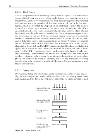
This is a simple method for patterning, usually metallic, layers. It is used for metals
that are difficult to etch or where etching might damage other materials already on
the substrate. A typical process is as follows. First, a resist is deposited and patterned
with an image where the areas intended to have metal are cleared by the developer.
Second, metal is deposited by evaporation or sputtering. Finally, the resist is
removed in a solvent such as acetone that takes away the resist and lifts off the
unwanted metal. For best results the developed pattern has undercut edges. This can
be achieved by soaking the resist in chlorobenzene. Depending on the exposure time,
this penetrates only a certain depth into the resist, causing the surface of the resist to
develop at a slower rate than the resist in contact with the wafer. The process, how-
ever, is difficult to control and success is often only partial. A better approach is to
use two different resists such as PMGI SF11 and a standard resist. In this process,
illustrated in Figure 2.8, the PMGI SF11 is deposited and flood exposed before the
application of a standard resist. After exposure with the pattern, the resist is devel-
oped. The PMGI SF11 develops at a faster rate than the standard resist, thereby leav-
ing an overhang. Other materials can be used in a liftoff process. For example, the
two layers of resist can be replaced by aluminum and polysilicon with orthophos-
phoric acid used both to create the overhang and to do the final liftoff. Providing
that the layer to be patterned is not chemically attacked by orthophosphoric acid,
the process will work.
2.3.2.5 Topography
Deep cavities etched into silicon are a common feature in MEMS devices, and ide-
ally, the processing steps to produce these are done at the end of the process. How-
ever, the design of the device may not always allow this, for example, when contact
Spin on PGMI resist
and flood expose
Spin on photoresist
and expose pattern
Develop pattern
in resist
Deposit metal
Lift off unwanted
metal by dissolving
resist in asolvent
Figure 2.8 Process flow for liftoff.