
Page 36 - MEMS Mechanical Sensors
P. 36
2.3 Fabrication Techniques 25
gradually exposed as the etch proceeds. Using the anisotropic etch property, various
shapes such as inverted pyramidal holes, V-shaped grooves, and flat bottomed
trenches with sidewalls sloping at 54.7 can be formed. If the edge of the window is
not in a {111} plane, then the mask is undercut and various crystal facets appear,
although, by etching for a sufficient length of time, these crystal facets will eventually
be eroded and a {111} plane will eventually be revealed. In addition to holes, silicon
structures bounded by the {111} planes can also be formed. These are usually in the
form of trapezoidal bosses bounded by the four {111} planes. In this case other crys-
tal planes are exposed where the {111} planes meet at the corners of the structure,
resulting in severe undercutting at these corners. By careful mask design, this under-
cutting can be avoided such that the corner of the boss is perfectly formed from two
{111} planes. This technique is called corner compensation and a number of different
patterns have been designed to achieve this [16, 17]. One of the simpler corner com-
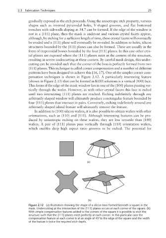
pensation techniques is shown in Figure 2.12. A particularly interesting feature
(shown in Figure 2.13) that can be formed in KOH solutions is a vertical {100} face.
This forms if the edge of the mask window lies in one of the {100} planes passing ver-
tically through the wafer. However, as with other crystal facets this face is etched
until two intersecting {111} planes are reached. Etching indefinitely through any
arbitrarily shaped window will ultimately produce a rectangular feature bounded by
four {111} planes that intersect in pairs. Conversely, etching indefinitely around any
arbitrarily shaped island feature will ultimately remove the feature.
In addition to {100} silicon wafers, it is also possible to obtain wafers with other
orientations, such as {110} and {111}. Although interesting features can be pro-
duced by anisotropic etching on these wafers, they are less versatile than {100}
wafers. A pair of {111} planes pass vertically through {110} orientation wafers,
which enables deep high aspect ratio grooves to be etched. The potential for
(a)
(b)
Figure 2.12 (a) Illustration showing the shape of a silicon boss formed beneath a square in the
mask. Undercutting at the intersection of the {111} planes occurs at each corner of the square. (b)
With simple compensation features added to the corners of the square it is possible to etch the
structure such that the {111} planes meet perfectly at each corner. In this particular case the
compensation feature at each corner is at an angle of 45°to the edge of the square and the width
of the feature is twice the required etch depth.