
Page 39 - MEMS Mechanical Sensors
P. 39
28 Materials and Fabrication Techniques
limitation can be overcome in design by avoiding large disparities in the feature sizes
on the mask.
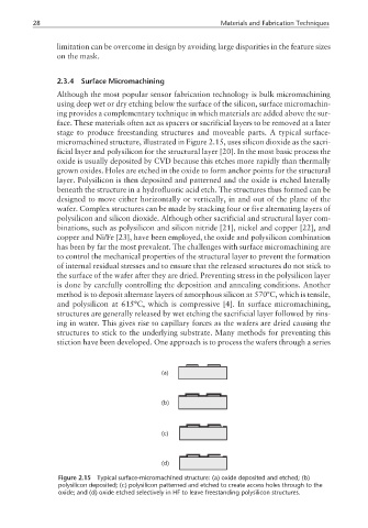
2.3.4 Surface Micromachining
Although the most popular sensor fabrication technology is bulk micromachining
using deep wet or dry etching below the surface of the silicon, surface micromachin-
ing provides a complementary technique in which materials are added above the sur-
face. These materials often act as spacers or sacrificial layers to be removed at a later
stage to produce freestanding structures and moveable parts. A typical surface-
micromachined structure, illustrated in Figure 2.15, uses silicon dioxide as the sacri-
ficial layer and polysilicon for the structural layer [20]. In the most basic process the
oxide is usually deposited by CVD because this etches more rapidly than thermally
grown oxides. Holes are etched in the oxide to form anchor points for the structural
layer. Polysilicon is then deposited and patterned and the oxide is etched laterally
beneath the structure in a hydrofluoric acid etch. The structures thus formed can be
designed to move either horizontally or vertically, in and out of the plane of the
wafer. Complex structures can be made by stacking four or five alternating layers of
polysilicon and silicon dioxide. Although other sacrificial and structural layer com-
binations, such as polysilicon and silicon nitride [21], nickel and copper [22], and
copper and Ni/Fe [23], have been employed, the oxide and polysilicon combination
has been by far the most prevalent. The challenges with surface micromachining are
to control the mechanical properties of the structural layer to prevent the formation
of internal residual stresses and to ensure that the released structures do not stick to
the surface of the wafer after they are dried. Preventing stress in the polysilicon layer
is done by carefully controlling the deposition and annealing conditions. Another
method is to deposit alternate layers of amorphous silicon at 570°C, which is tensile,
and polysilicon at 615°C, which is compressive [4]. In surface micromachining,
structures are generally released by wet etching the sacrificial layer followed by rins-
ing in water. This gives rise to capillary forces as the wafers are dried causing the
structures to stick to the underlying substrate. Many methods for preventing this
stiction have been developed. One approach is to process the wafers through a series
(a)
(b)
(c)
(d)
Figure 2.15 Typical surface-micromachined structure: (a) oxide deposited and etched; (b)
polysilicon deposited; (c) polysilicon patterned and etched to create access holes through to the
oxide; and (d) oxide etched selectively in HF to leave freestanding polysilicon structures.