
Page 42 - MEMS Mechanical Sensors
P. 42
2.3 Fabrication Techniques 31
V
Glass
Silicon
Hotplate
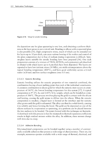
Figure 2.16 Setup for anodic bonding.
the deposition rate for glass sputtering is very low, and obtaining a uniform thick-
ness as the layer grows is not a trivial task. Bonding to silicon with evaporated glass
is also possible [35]. High compressive stress, much of which can be annealed out
for layers up to 10 µm thick, can cause serious bowing of the wafers and control of
the glass composition due to loss of sodium during evaporation is difficult. Spin-
on-glass layers suitable for anodic bonding have been prepared [36]. One such
preparation consists of a mixture of TEOS, MTEOS, and a potassium salt dissolved
in ethanol with which layers up to 6 µm thick have been deposited. The layers are
reported to have low intrinsic stress (30 MPa), are stable at temperatures above the
typical bonding temperature (420°C), and have good uniformity across a 6-inch
wafer (±20 nm) and low surface roughness (rms: 0.5 nm).
2.3.5.3 Eutectic Bonding
Eutectic bonding utilizes the eutectic properties of two materials combined, the
combination having a lower melting point than each of the individual constituents.
A common combination is silicon-gold for which the eutectic state occurs at a tem-
perature of 363°C, the lowest bonding temperature for this system [37]. A typical
composition is 97.1% Au and 2.85% Si by weight, which can be bonded at a tem-
perature of 386°C. The process involves placing the gold in contact with the silicon
and heating, causing the gold atoms to diffuse into the silicon. When the eutectic
composition is reached, a liquid layer is formed at the interface and the eutectic
alloy grows until the gold is exhausted. The alloy can then be cooled slowly, causing
it to solidify and hence forming the bond. The gold can be deposited on one of the
silicon surfaces by evaporation or sputtering, or a preform can be placed between
the two surfaces to be bonded. The joints formed with this technique are hermetic.
A drawback with this process is that the mismatch in thermal expansion coefficients
results in high residual stresses within the alloy. In addition, these stresses change
with time due to creep.
2.3.5.4 Adhesive Bonding
Micromachined components can be bonded together using a number of commer-
cially available adhesives that possess a wide range of characteristics. There are, for
example, numerous epoxies available with a wide range of thermal, electrical, and