
Page 46 - MEMS Mechanical Sensors
P. 46
2.3 Fabrication Techniques 35
2.3.9 Porous Silicon
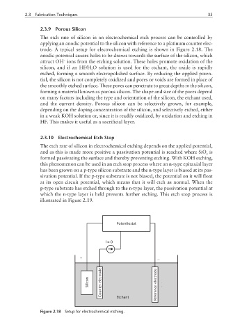
The etch rate of silicon in an electrochemical etch process can be controlled by
applying an anodic potential to the silicon with reference to a platinum counter elec-
trode. A typical setup for electrochemical etching is shown in Figure 2.18. The
anodic potential causes holes to be drawn towards the surface of the silicon, which
−
attract OH ions from the etching solution. These holes promote oxidation of the
silicon, and if an HF/H O solution is used for the etchant, the oxide is rapidly
2
etched, forming a smooth electropolished surface. By reducing the applied poten-
tial, the silicon is not completely oxidized and pores or voids are formed in place of
the smoothly etched surface. These pores can penetrate to great depths in the silicon,
forming a material known as porous silicon. The shape and size of the pores depend
on many factors including the type and orientation of the silicon, the etchant used,
and the current density. Porous silicon can be selectively grown, for example,
depending on the doping concentration of the silicon, and selectively etched, either
in a weak KOH solution or, since it is readily oxidized, by oxidation and etching in
HF. This makes it useful as a sacrificial layer.
2.3.10 Electrochemical Etch Stop
The etch rate of silicon in electrochemical etching depends on the applied potential,
and as this is made more positive a passivation potential is reached where SiO is
2
formed passivating the surface and thereby preventing etching. With KOH etching,
this phenomenon can be used in an etch stop process where an n-type epitaxial layer
has been grown on a p-type silicon substrate and the n-type layer is biased at its pas-
sivation potential. If the p-type substrate is not biased, the potential on it will float
at its open circuit potential, which means that it will etch as normal. When the
p-type substrate has etched through to the n-type layer, the passivation potential at
which the n-type layer is held prevents further etching. This etch stop process is
illustrated in Figure 2.19.
Potentiostat
I=0
+
−
electrode electrode
Silicon
Counter Etchant Reference
Figure 2.18 Setup for electrochemical etching.