
Page 45 - MEMS Mechanical Sensors
P. 45
34 Materials and Fabrication Techniques
achieved with such UV-LIGA processes are much less than 10:1. For example, using
the UV-sensitive negative resist, PMER N-CA3000, near vertical sidewalls with an
aspect ratio of the order of 6:1 and resist several tens of microns thick have been
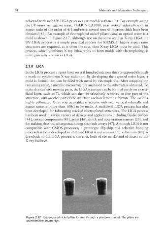
obtained [43]. An example of electroplated nickel pillars using an optical resist as a
mold is shown in Figure 2.17. Although not on the same scale as X-ray LIGA the
UV-LIGA process is a simple practical process for MEMS. If higher aspect ratio
structures are required, as is often the case, then X-ray LIGA must be used. This
process, which combines X-ray lithography to form molds with electroplating, is
more generally known as LIGA.
2.3.8 LIGA
In the LIGA process a resist layer several hundred microns thick is exposed through
a mask to synchrotron X-ray radiation. By developing the exposed resist layer, a
mold is formed that can be filled with metal by electroplating. After stripping the
remaining resist, a metallic microstructure anchored to the substrate is obtained. To
make devices with moving parts, the LIGA structure can be formed partly on a sacri-
ficial layer, such as Ti, which can then be selectively removed to free part of the
structure, with another part of the structure anchored to the substrate. The use of a
highly collimated X-ray source enables structures with near vertical sidewalls and
aspect ratios of more than 100:1 to be made. A multilevel LIGA process has also
been developed for fabricating stacked electroplated structures. The LIGA process
has been used in a wide variety of devices and applications including fluidic devices
[44], optical components [45], gears [46], shock and acceleration sensors [23], and
for making electrodischarge machining electrode arrays [47]. Although LIGA is not
compatible with CMOS processes, a prototype flip-chip and selective bonding
process has been developed to combine LIGA structures with IC substrates [48]. A
drawback to the LIGA process is the cost, both of the masks and of access to the
X-ray facilities.
Figure 2.17 Electroplated nickel pillars formed through a photoresist mold. The pillars are
approximately 20 µm high.