
Page 47 - MEMS Mechanical Sensors
P. 47
36 Materials and Fabrication Techniques
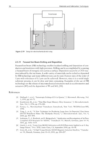
Potentiostat
I=0
+ −
electrode electrode
n-Si Counter Reference
p-Si Etchant
Figure 2.19 Setup for electrochemical etch stop.
2.3.11 Focused Ion Beam Etching and Deposition
Focused ion beam (FIB) technology enables localized milling and deposition of con-
ductors and insulators with high precision. Milling can be accomplished by scanning
a focused beam of energetic ions across a surface. Deposition occurs by a CVD reac-
tion induced by the ion beam. A wide variety of materials can be etched or deposited
by FIB technology and many different ions can be used. Feature sizes of the order of
1 µm with tolerances of 0.1 µm can be achieved. However, since it is a serial single
substrate process, it can be slow and time consuming. Examples of the use of FIB
technology are the release of micromechanical structures such as accelerometers and
actuators [49] and the deposition of W and SiO [50].
2
References
[1] Hedlund, C., et al., “Anisotropic Etching of Z-Cut Quartz,” J. Micromech. Microeng., Vol.
3, 1993, pp. 65–73.
[2] Kruelevitch, M., et al., “Thin Film Shape Memory Alloy Actuators,” J. Microelectromech.
Syst., Vol. 5, 1996, pp. 270–282.
[3] Kovacs, G., Micromachined Transducers Sourcebook, New York: WCB/McGraw-Hill,
1998.
[4] Yang, J., et al., “A New Technique for Producing Large-Area As-Deposited Zero-Stress
LPCVD Polysilicon Films: The Multipoly Process,” J. Microelectromech. Syst., Vol. 9,
2000, pp. 485–494.
[5] Seideman, V., S. Bütefisch, and S. Büttgenbach, “Application and Investigation of In-Plane
Compliant SU8-Structures for MEMS,” Transducers ’01, Munich, Germany, June 10–14,
2001, pp. 1616–1619.
[6] Daniel, J., et al., “Large Area MEMS Fabrication with SU8 Photoresist Applied to an X-Ray
Image Sensor,” Proc. SPIE, Santa Clara, CA, September 2000, pp. 40–48.
[7] Köser, H., et al., “A High Torque Density MEMS Magnetic Induction Machine,” Transduc-
ers ’01, Munich, Germany, June 10–14, 2001, pp. 284–287.